The IP vendor #1, leading the pack with revenues more than twice the closest competitor revenues, has to position on the new IoT market, especially because ARM’s main product line is processor IP family, and MCU or CPU is certainly at the earth of the SmarCoT: the “Smart” part. In fact, ARM’s customers have the freedom to develop any… Read More
 The Accidental Infrastructure: How Crypto Miners Built the Foundation of the AI BoomMost crypto forty-niners died broke in a warehouse…Read More
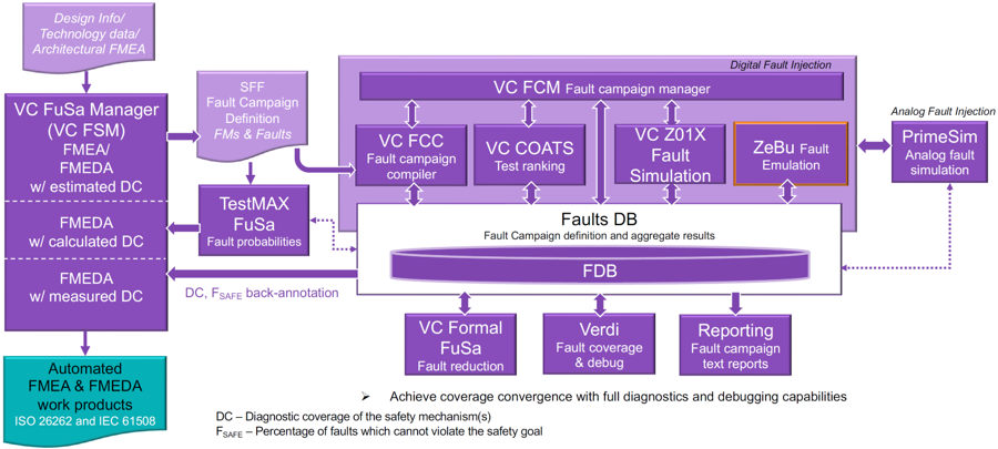 From Detection to Safety: Reframing Fault Simulation for Functional SafetyIn the early 1980s, when computer-aided engineering (CAE),…Read More
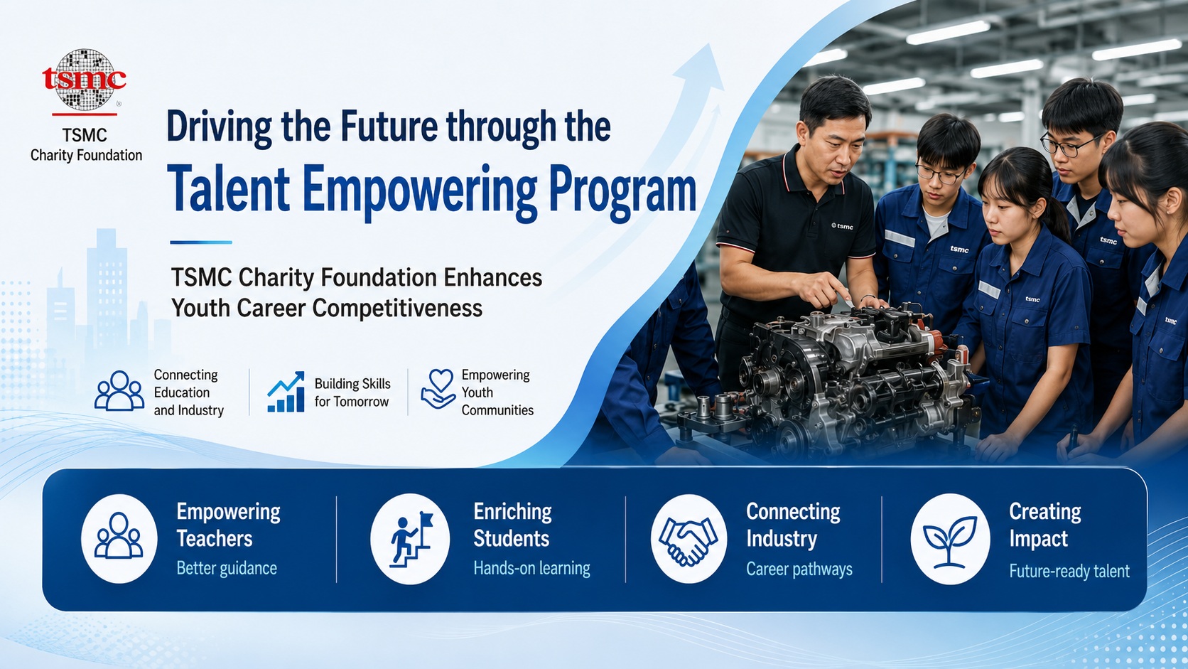 Driving the Future through the “Talent Empowering Program”: Why TSMC Charity Foundation’s Youth Career Initiative MattersThe future of work will not be shaped…Read More
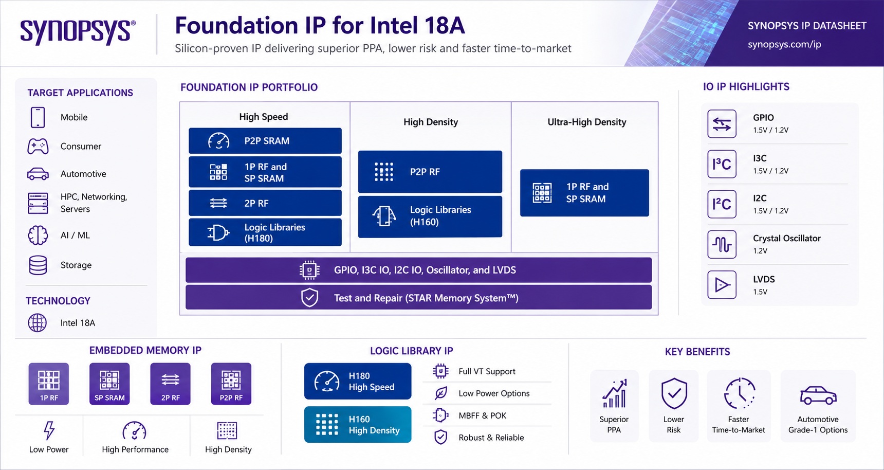 Foundation IP for Intel 18A: Technical Overview and Why It MattersSynopsys Foundation IP for Intel 18A is a…Read More
 WEBINAR: Defacto is Boosting Front-end SoC Design With AI-Powered EDA toolsThe real promise of AI in EDA is…Read More
Global Foundries and IBM, More Details
Now that the dust has started to settle on the GlobalFoundries acquisition of IBM’s semiconductor business it is possible to look into another level of detail about what GlobalFoundries will be acquiring in the way of technology and IP. Of course, the deal hasn’t formally closed yet so this won’t all happen … Read More
HLS Tools Coming into Limelight!
For about a decade I am looking forward to seeing more of system level design and verification including high level synthesis (HLS), virtual prototyping, and system modeling etc. to come in the main stream of SoC design. Although the progress has been slow, I see it accelerating as more and more tools address the typical pain points… Read More
Using HAPS-DX for system-level deep trace debug
Debugging an ASIC design in an FPGA-based prototyping system can be a lot like disciplining a puppy. If you happen to be there at the exact moment the transgression occurs and understand what led up to that moment, administering an effective correction might be possible.
Catching RTL in the act requires the right tools. Faults in… Read More
Don’t be an “ID-IoT”
Let’s just come out and say it: Not using the most robust security to protect your digital ID, passwords, secret keys and other important items is a really, really bad idea. That is particularly true with the coming explosion of the Internet of Things (IoT).
The identity (i.e. “ID”) of an IoT node must be authenticated and trusted … Read More
Is Your Washing Machine a Connected Thing?

In fact the question could be about your watch, thermostat or other smart appliance, as soon as the “thing” relies on one or more sensors to function. In this case, we are close to call this thing an IoT (or SmarCoT), we just need to add WiFi, BTLE, ZigBee connectivity. Sensors are ubiquitous, integrated into smartphone, automotive,… Read More
Qualcomm Enters Server CPU Market
Fresh from the leaked memo that Intel is merging its mobile business into its PC client group, Qualcomm is going the other way and has confirmed that it is entering the ARM server CPU market, an announcement made at its analyst day earlier today.
This is a major trend that less than a month ago I reported from the Linley microprocessor… Read More
MIPS CPU and Newton2 Platform for Wearables
I have written recently about SmarCoT (Smart Connected Thing) and smartwatches are one of these numerous smart and connected applications that some still refer to as IoT. Imagination Technologies is working hard to be part of the SmarCoT ecosystem and Ingenic, IMG customer, has recently launched a MIPS-based chip (M200) and … Read More
Atmel, IoT and CryptoAuthentication
One of the companies that is best positioned to supply components into the IoT market is Atmel. For the time being most designs will be done using standard components, not doing massive integration on an SoC targeted at a specific market. The biggest issue in the early stage of market development will be working out what the customer… Read More
Arteris on a winning streak in 2014
When Arteris sold key network-on-chip intellectual property and most of its human assets to Qualcomm earlier this year, it was big news. We suggested the bigger news after a restaffing effort would be a next-generation NoC release, and a new round of design wins.
Some developments were already in the pipeline. … Read More
Consolidation and Competition: Who is Winning the $4.5 Billion Interface IP Race?