Reconfigurable computing began with FPGA cards dropped into expansion slots in workstations. FPGA-based prototyping vendors tended away from that model as interconnect speeds rose and cabling complexity between modules increased. Much faster PCIe interfacing and bigger FPGAs mean revisiting the concept.… Read More
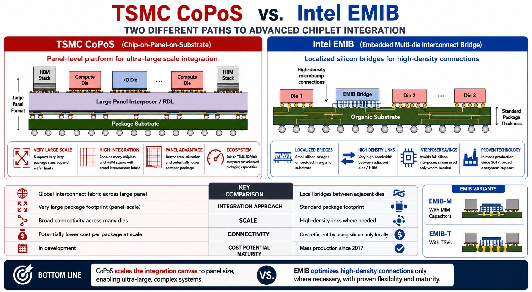 TSMC CoPoS Versus Intel EMIB Semiconductor PackagingTSMC’s CoPoS, generally described as Chip-on-Panel-on-Substrate, and Intel’s…Read More
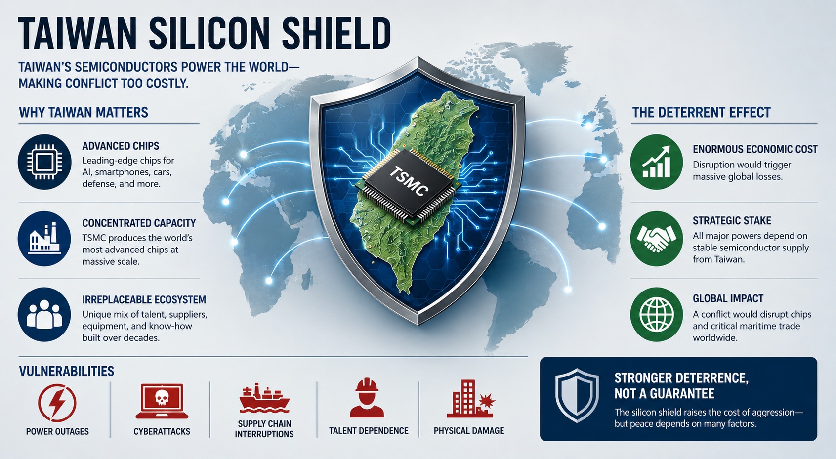 The Silicon Shield Has Never Been Stronger!The “Silicon Shield” describes the idea that Taiwan’s…Read More
 Agentrys Designs a Real Chip with its Multi-Agent WorkforceThe face of EDA is changing. For forty…Read More
 Must-See DAC Panel – Build vs Buy: Who Owns the Intelligence Behind Tomorrow's Chips?This year, DAC will be buzzing about AI…Read More
Synopsys at DVCon 2016

It’s that time of year again – DVCon starts on Monday Feb 29[SUP]th[/SUP] and as always should be a packed event. Synopsys plans a big showing, in the exhibit hall, in a sponsored lunch, at tutorials and in papers. Time to get your conference shoes on and go check them out – I plan to be there all week.
One of the most obvious things you will… Read More
Should terrorists prefer iPhone (thanks to privacy)?
The case between Apple and the FBI may not be as limpid as it could be. If you ask me if Apple, or any US or Europe based supplier of high tech system should help the FBI (or any similar organization) and provide the technical support needed to extract information belonging to a terrorist, my answer would be definitely YES.
I don’t know… Read More
TSMC and Intel on the Long Road to EUV
Today is the first day of the SPIE Advanced Lithography Conference and Extreme Ultraviolet (EUV) updates were a big focus.… Read More
SoC power management a study in transition latency
Apple’s recent bout with ‘Batterygate’ highlighted just how important dynamic power management can be. Our last Sonics update looked at using their NoC to manage power islands; this time, we look at their research progress on architectural measures for power management.… Read More
A Brief History of Open-Silicon
In 2003, when Open-Silicon was founded there was a growing need for flexible and innovative ways of getting chip designs manufactured. Semiconductor companies, given the alternatives of COT or traditional ASIC, often were looking for more flexibility without the huge investment and risk of going COT. Let’s look at how Open-Silicon… Read More
FinFET For Next-Gen Mobile and High-Performance Computing!
Evolving opportunities call for new and improved solutions to handle data, bandwidth and power. Moving forward, what will be the high-growth applications that drive product and technology innovation? The CAGRs for smartphone and data center continue to be very strong and healthy. … Read More
Advanced Micro Device’s New Polaris FinFET-Based Architecture Could Open New Doors
It seems of late like there is an unlimited thirst for GPU performance at the right power efficiency. Whether it is deep learning, object recognition, artificial intelligence, simulations, VR or AR, the industry desperately needs GPU improvements. Many within the graphics industry would agree that a new era of graphics performance… Read More
How to handle petabyte-scale traffic growth?
If you search the web for IP traffic growth, you will find many graphics, but the common result is that IP traffic is growing with high CAGR for many years and will again continue to grow with such high CAGR for the next five years. For example the global mobile data traffic is expected to grow with 53% CAGR 2015-2020… even if the smartphone… Read More
Emerging Smartphone Display Insights from Patents
US201403549 illustrates a display that includes the multifunctional pixels. Each multifunctional pixel can include several display areas as well sensors. Combining visual display technology with sensors provides the touchscreen operation by use of a finger, stylus or other object positioned on or near the visual display,… Read More
Enhancing Multi-Domain System Simulation with FMI Co-Simulation