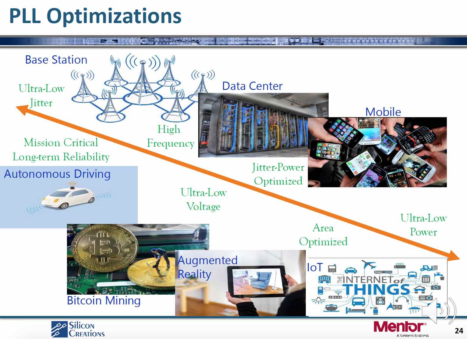
TSMC’s Open Innovation Platform’s main objective is to create and promote partnership for producing chips. This year’s OIP event included a presentation on the joint efforts of Silicon Creations, Mentor, a Siemens business and TSMC to produce essential PLL IP for 5nm and 3nm designs. The relentless push for smaller geometries has created huge challenges for all kinds of designs but have pushed analog blocks further than ever. Mentor and Silicon Creations presented the results for 5nm and 3nm PLLs, which are critical IP for any digital or analog design. In particular large high speed SoCs live or die on PLL performance.
PLLs are some of the highest volume analog IPs. Silicon Creations’ PLL TS28HMP FRAC is used on 140 different production chips accounting for an incredible instance count of over one billion. Achieving the reliability necessary for those volumes while meeting increasingly tighter specifications and with the compounding difficulties of shrinking process geometry is no small feat.

No matter how good Silicon Creations’ design team is, they simply could not get their widely used IP out the door without the efforts of Mentor and TSMC. Mentor has contributed to this success with their innovative Analog FastSPICE (AFS) Platform. TSMC, in addition to their advanced fabrication capabilities, provide silicon accurate models for cells, devices and interconnect.
I have written previously about Silicon Creations’ advanced process node IP as they were heading into 5nm. They reported first pass silicon success at 5nm and several active projects in flight for 3nm. Silicon Creations has been TSMC’s Mixed Signal Partner of the Year from 2017 to 2019.
So, what are the specific challenges that come with moving further along from 5nm to 3nm? The number of GDS layers needed has increased 9X since 180nm. The Design Rule Manual has increased an order of magnitude from 180nm to 3nm. Consequently, DRC runs are now 100X longer at 5nm than at 180nm. So, clearly process complexity is a real issue.
Well, does analog scale in a way anything like digital? According to the presentation, it does scale, but not nearly as handily as digital. Expect to see a 10X reduction in area compared to the 1000X seen in digital in going from 180nm to 3nm. In looking at the graph provided it looks like there is a local minimum around 7nm, so the future of scaling will be interesting to see.
The real fly in the ointment is interconnect, which is becoming an extremely important limiting factor for analog designs at 3nm. From 40nm to 3nm relative wire resistance (Ohms/sq) has risen almost an order of magnitude. TSMC is working to relieve the pressure on designers, but the issue will never entirely go away. Now, even early functional verification simulations need to account for parasitics. This is pushing simulation times up at an incredible rate. The effects of this include longer development cycles and the need for more simulation licenses. The presentation offers some hope through the effective RC reduction found in AFS.
Another source of pain for simulation is the large range of time scales that must be looked at to verify a design. From the ~100fs scale of jitter requirements to the ~1ms time required to analyze link requirements, the scope of timeframes ranges almost 10 orders of magnitude. Also, many analog subsystems require extensive simulation to ensure proper operation. Some examples that were provided include digital spread spectrum modulation, digital jitter cleaner, fast hopping FLL for DFS, phase alignment, and fractional LC PLL with noise cancellation.
Silicon Creations talked about how they rely on the many advanced features of Mentor’s AFS Platform to get through the simulation process. They report that they see good correlation with AFS and silicon measurement. They included graphs comparing simulation and silicon measurements for phase noise at 5nm, IoT PLL fast locking, oscillator frequency stability and transient noise.
The papers at TSMC’s OIP event are usually pretty comprehensive and interesting. This one was no exception. It also goes into detail on the Silicon Creations compute farm, PLL applications, and several other aspects of their verification flow. There is interesting detail about the complete AFS platform as well. I highly suggest viewing the presentation replay.
Also Read:
Essential Analog IP for 7nm and 5nm at TSMC OIP
Keeping Pace With 5nm Heartbeat
Context is Everything – especially for autonomous vehicle IP
Share this post via:


Comments
There are no comments yet.
You must register or log in to view/post comments.