Connecting “things” to the Internet and enabling sensing and remote control, data gathering, transmission, and analysis improves many areas: safety and quality of life, healthcare, manufacturing and service delivery, energy efficiency, and the environment. The concept of the Internet of Things (IoT) is quickly becoming a reality. At this year’s IDC Smart TECHnology Conference, attendees learned that IoT connected devices could number 50 billion by 2020 and the data generated by these devices could reach 50 trillion gigabytes. Clearly, there is significant opportunity for system and semiconductor companies developing the connected technologies that are fueling this space.
A typical IoT node integrates one or multiple sensors, analog front-end (AFE) modules, micro-electro-mechanical systems (MEMS), analog-to-digital converters (ADC), communication interfaces, wireless receivers/transmitters, a processor, and memory. Therefore, the system on chip (SoC) embodying the IoT node function is a microcontroller integrated with analog peripherals, creating an inherently mixed-signal design. To design SoCs for IoT applications in a competitive landscape where differentiation in features and price is critical, designers must address some key challenges, including:
- Integration of analog and digital functions
- Software-hardware verification
- Power consumption
Low Power: How Low Can You Go?
Power consumption is one of the most critical considerations for IoT applications because the devices typically operate on batteries for many years, ideally recharging by harvesting energy from the environment. To minimize power consumption, designers choose power-efficient processors, memory, and analog peripherals, and optimize the system such that only the necessary parts operate at a given time, while the rest of the system remains shut down. For example, consider a device that senses pressure—if there are no changes, only the peripheral monitoring sensor is powered on until a pressure change is detected, awaking the rest of the system to process the information and send it to the host. Another example is a smart meter. Most of the time, this type of device will be in standby mode, waking up every so often to collect power usage data and sending this data perhaps once daily to the power company. Some parts of the design are off, others are on. There might be about a dozen different modes of operation within the system, and all of them need to be verified.
To optimize power consumption, designers use many different techniques, including multiple supply voltages, power shutoff with or without state retention, adaptive and dynamic frequency scaling, and body biasing. In a pure digital design, implementation and verification of these low-power techniques are highly automated in a top-down methodology following common power specifications.
Analog content in IoT devices represents more challenges since it is usually implemented bottom up without explicit low-power specifications, leaving transistor-level simulation as the only verification option. Cadence has automated mixed-signal simulation using Common Power Format (CPF) for specifying behavior at crossing between analog and digital domains in case of power domain changes and power shut-offs. Furthermore, Cadence® Virtuoso® Schematic Editor is able to capture power intent for a custom circuit and export it in the CPF format for static low-power verification. The static method is much faster than simulation for discovering common low-power errors, like missing level shifters or isolation cells.
Hardware-Software Verification
Software plays a crucial role in IoT devices as sensor controls, data processing, and communication protocols are functions often implemented in software. Therefore, system verification must include both software and hardware. To reduce verification time, it is important to start software and hardware development and verification in parallel. For example, instead of waiting for silicon, software development and debugging should start earlier using a virtual prototyping methodology. Cadence Virtual System Platform provides the capability to create virtual models and integrate them into a virtual system prototype for early system verification, software development, and debugging.
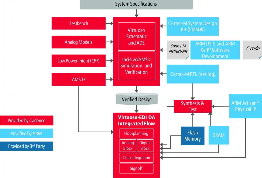
When it comes to systems including analog, Cadence offers some unique capabilities. Incisive® Enterprise Simulator is capable of simulating an entire system, including register-transfer level (RTL), for a processor with a compiled instruction set, digital block in RTL, and analog modeled using real number models. This enables hardware and software engineers to start collaborating sooner on developing software and hardware concurrently, instead of sequentially.
High Level of Integration
To ease the development process and shorten the design cycle for IoT devices, designers re-use intellectual property (IP) blocks for a variety of functions. They either design these IP blocks in house, or acquire them from outside vendors, so they can focus on a few differentiating blocks and on integration. Getting the SoC integrated quickly and cost-effectively is the key to success.
Integrating analog IP requires special care. To verify system functions properly in all possible scenarios, designers use simulation. Simulating analog parts at the transistor level, although necessary for some aspects of performance verification, is not the most efficient method to incorporate analog into SoC functional verification. Cadence has developed a methodology based on very efficient real number models (RNM) for abstracting analog at a higher level and for SoC verification without a major performance penalty. Automated model generation and validation capabilities in the Virtuoso platform assist designers in overcoming traditional modeling challenges and taking advantage of simulation using RNM supported in Verilog-AMS or recently standardized System Verilog, IEEE1800 extensions.
Using RNM, designers can validate functionality of the design in many different scenarios more thoroughly and much faster, and leave only specific performance verification to transistor-level simulation.
Once an IoT design is verified, it is important to realize it in silicon, productively. To ensure design convergence throughout the physical implementation process, analog and digital designers must closely collaborate on deriving an optimal floorplan, full-chip integration, and post-layout performance and physical signoff. Cadence integrated its leading Virtuoso analog and Encounter® digital platforms on the industry-standard OpenAccess database to provide a unified flow for mixed-signal designs. The flow operates on the common database for analog and digital that requires no data translation and enables easier iteration between analog and digital designers in optimizing the floorplan, implementing engineering change orders (ECOs), and performing full-chip integration and signoff.

Summary
The modern world will continue to get more connected, and the electronic products that make this possible, smarter. This creates not only more challenges but more opportunities for design engineers creating the complex SoCs that power these smart, connected products. Processors, analog components, IP blocks, tools, and methodologies all play important roles in addressing power, integration, and price challenges. With the right design solutions, engineers can deliver differentiated products that support what some experts say is a key enabler of the fourth industrial revolution: the Internet of Things.
By Mladen Nizic, Engineering Director, Mixed-Signal Solutions, Cadence
lang: en_US
Share this post via:


Comments
There are no comments yet.
You must register or log in to view/post comments.