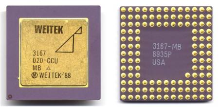
During last week-end, I had the good surprise to meet with one of my oldest friend, Eric, who remind me the old time, when we were working together as ASIC designers for… a Supercomputer project.
In France, in a French company (Thomson CSF) active in the military segment and being able to spend which was at that time a fortune ($25M) to develop a supercomputer from scratch, and when I say from scratch, that mean that we had to invent almost everything, except the ASIC design methodology and the EDA tools, both being provided by VLSI Technology Inc. To be honest, we have been very lucky that a French solution (like Matra Harris Semiconductor or Thomson Composant Speciaux) had not be chosen, which could have happened for obscure political reasons. We had in our hands which were considered as the Rolls Royce for ASIC designers in 1987: all the design team was equipped with SUN workstation, and the design tool set from VLSI was really user friendly… except it was missing a synthesis tool, but none of us knew Synopsys, this obscure start-up, so we were pretty happy to start. Just for your information, I will describe what was the type of work done by a two engineer team during a 18 month period.
Just a word about the project itself. The supercomputer chief architect was a talented University Professor, talented but this was his first contact with the industrial world. He had defined the machine architecture, based on three main areas: the CPU boards (based on off-the-shelf CPU chips, Weitek Abacus), the FIFO based interconnects network and the memory area, as well as six different ASIC devices. It was a “superscalar” architecture. The task I was assigned with Eric was to design all the function which will be reused by the different ASIC designs: the FIFO, the Test functions and the Clock distribution inside the chips.

The first one was the easier, as we had to define the specification of a FIFO compiler, the compiler itself being a full custom design, at transistor level, would be subcontracted by VLSI Technology. We just took a pen and a paper and defined the memory point, transistor by transistor, and the FIFO behavior… in written. No simulations (SPICE was not part of our EDA package), just discussion with Michel Gigluielmetti, our interface at VLSI. VLSI was in charge of the compiler design and model generation, as we had to be able starting to design and integrate FIFO far away before seeing any working Silicon. When I look back, it was pretty risky, isn’t it?
The Test Strategy was based on the newly introduced JTAG IEEE 1149.1 for « Standard Test Access Port and Boundary-Scan Architecture », this part was not that difficult, as everything was defined in the standard.
Then, we looked at the Clock distribution. Remember, it was in 1987, there was no Clock Distribution Macro” that we could use. The Clock was a magic signal, running at 20 MHz (such a high speed!), that designers were using to run their simulations, a perfect signal with no skew… How to manage the clock distribution in a chip counting 2 or 3,000 Flip Flops? Starting inside the chip, we then thought about the inter chip communications, and drop a couple of equations… and discovered that we had a real issue here! How will the entire system works, with chips communicating from board to board which could be located at one meter from each other? What about the fly time within interconnect? And so on… The most surprising is that we (two beginners) discover this issue, and that none of the seasoned engineers working at a higher management level did not even thought about it!
So Eric and I send a note, copying all the management, to raise the issue. Then started one of the most amazing, creative time, after the project leader decided to assign us to work full time on the clock distribution within the machine, inside and outside the ASIC. At first, define the basic equations:
When you send a data from a “slow” device, you have to comply with:
Temission_slow + Tinterconect + Tset-up + Skew < Clock_cycle
But, when the emitter is “fast”, the equation becomes:
Temission_fast + Tinterconnect > Thold + Skew
This is at that step that we have discovered that two identical ASIC devices could exhibit variations from 1 to 3, when taking into account the voltage, process and temperature induced variations! Our managers guess what it was 10 or 20%… So we defined the clock distribution in the machine, selecting external buffers as fast as possible (for the minimum transit time, the specification was… 0ns), trying to minimize the impact of the buffering. But when doing this, we realize that it could not work for any case, even if we increase the clock period (and decrease the frequency, which was not really what you want to do when you design a supercomputer…). With the help of VLSI technology, we defined a kind of Digital Lock Loop (DLL), in order for the ASIC to self calibrate (a fast device would delay the time at which the data was emitted, to guarantee the hold time). We also defined different phase for the clock period, so we could artificially enlarge the clock cycle, to receive the data with no set-up problem. In other words, we had to invent the wheel, even if I am sure that the designers working at Cray Research did it before us! When I see the size of a team working today on a single device (OMAP5 or equivalent), I think we were very lucky to discover the ASIC design in such a way.
Because there is a moral in every story, I must say that the project was suddenly ended by Thomson CSF top management, when it appeared that the machine would never work, at least at 20 MHz, the official reason being the difficulties from Weitek to ship the CPU. Then, the Engineering manager of the software team moved to another Thomson’ subsidiary, in charge of developing tools for the stock market. Eric moved to Australia for one year, to learned surf. By the way, he is still living there! As far as I am concerned, I stayed in ASIC design, doing chips for Aircraft motors or Analogue simulation for the TGV and finally was ASIC FAE for TI, where my largest customer was Advanced Computer Research Institute (ACRI) designing… a supercomputer! But that is another story…
By Eric Esteve


Silicon Insurance: Why eFPGA is Cheaper Than a Respin — and Why It Matters in the Intel 18A Era