The semiconductor analysts are at it again, revising numbers, polishing their guesstimates, and patting each other on the back for being equally as inaccurate. I blame these crystal ball hacks for the semiconductor shortages and price hikes we are experiencing today.
These people get paid to guide investors, and the industry as a whole, to prevent chaos and catastrophe and they have failed us all. Last year semiconductor related manufacturing facilities went dark, people lost jobs, capacity expansion plans were put on hold. It will take years to recover the stability required for a healthy semiconductor growth cycle.

“All signs point to another semiconductor downturn as there have now been signs of softening demand from approximately 65 percent of total semiconductor demand,” wrote Christopher Danely, an analyst at J.P. Morgan, in a report circulated Wednesday (Aug. 18).
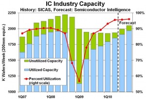
Danely also said semiconductor stocks peaked in 2Q10 and he expects utilization rates will peak in 3Q10.Why trust an analyst from a financial services firm that may or may not be short on semiconductor stocks? This is deja vu of my blog “Colossal Failure of Common Sense”, where these dirty scoundrels nearly bankrupted us, stealing our home equity, all while taking home million dollar bonuses, but I digress.

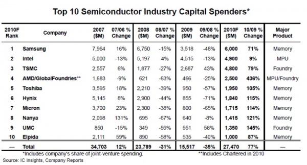
The most recent post by Bill Jewell at Semiconductor Intelligence suggests capacity utilization will continue to increase through the rest of the year, hitting 96 percent in the fourth quarter. I’m with Bill on this one. Capacity has still not rebounded from the 2009 fiasco but with the most recent semiconductor capital expenditures you can bet it will, with a vengeance:
[LIST=1]
As compared to numbers reported by iSupply earlier this year:

The capacity numbers that interest me the most are the 300mm fabs at 65nm and below, that is where the billions of dollars of capital expenditures are going. 300mm manufacturing technology is where the smartphone and other key enabling semiconductor technology comes from. At 300mm, UMC and TSMC are both running at 100% and will continue to do so for the next year or two as these are the same fabs that produce 40nm and 28nm. Both UMC and TSMC have increased 300mm production this year due to efficiencies and existing expansion projects. TSMC will also complete their 3rd GigaFab (FAB 15) next year. Global Foundries 300mm Fabs (1,7,8) will see increases this year of 20%. With additional expansions and the new 300mm fab in New York, GFI should break 2M 300mm wafers per year by 2015.
The questions I have are:
[LIST=1]
Rather than ask the so called experts I would rather hear it from the people who actually design and manufacture semiconductors. When I Google search, I always read the Wikipedia entry first, trusting the collective wisdom of millions versus a biased person who stole my home equity.
lang: en_US
Share this post via:


Is Intel About to Take Flight?