Everyone knows Moore’s Law: the number of transistors on a chip doubles every couple of years. We can take the process roadmap for Intel, TSMC or GF and pretty much see what the densities we will get will be when 20/22nm, 14nm and 10nm arrive. Yes the numbers are on track.
But I have always pointed out that this is not what drives the semiconductor industry. It is much better to look at Moore’s Law the other way around, namely that the cost of any given functionality implemented in semiconductors halves every couple of years. It is this which has meant that you can buy (or even your kid can buy) a 3D graphics console that contains graphics way beyond what would have cost you millions of dollars 20 years ago in a state of the art flight simulator.
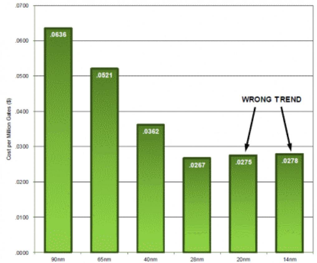
But look at this graph:
This shows the cost for a given piece of functionality (namely a million gates) in the current process generation and looking out to 20nm and 14nm. It is flat (actually perhaps getting worse). This might not matter too much for Intel’s server business since those have such high margins that they can probably live with a price that doesn’t come down as much as it has done historically. And they can make real money by putting more and more onto a chip. But it is terrible for businesses like mobile computing that don’t live on the bleeding edge of the maximum number of transistors on a chip. If you are not filling up your 28nm die and a 20nm die costs just the same (and is much harder to design) why bother? Just design a bigger 28nm die (there may be some power savings but even that is dubious since leakage is typically an increasing challenge).
If this graph remains the case, then Moore’s Law carries on in the technical sense that you can put twice as many transistors on your chip if you can think of something clever to do with them and can find a way to keep enough of them powered on. But it means there is no longer an economic driver to move to a new process unless you have run out of space on the old one.
Since EDA mostly makes money on designs in new processes (because they need new tools which can be sold at a premium) this is bad for EDA. It actually doesn’t make money on the first few designs coming through a new process because there is so much corresponding engineering to be done. But if the mainstream never moves, the cash-cow aspect of selling EDA tools to the mainstream won’t happen. And just like there is no business selling “microprocessor design tools” since there are too few groups who would buy them and their needs are too different, there might never be a big enough market for “14nm design tools” to justify the investment.
So that’s why this is the scariest graph in EDA.
Share this post via:


Musk’s Orbital Compute Vision: TERAFAB and the End of the Terrestrial Data Center