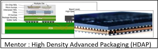
 Thursdays at the Design Automation Conference (DAC) are always a good time to catch up on areas of technology which are adjacent to that which you normally work. The exhibit floor is over and you have more time to spend in seminars. At this year’s DAC, I took advantage of a half day seminar put on by Mentor, a Siemens business, entitled High Density Advanced Packaging Trends. While this seminar was focused on electronic systems packaging, my work with integrated photonics has been clearly pointing to the need for system-in-package (SiP) solutions and I was interested to get a snapshot on the current state-of-the-art for IC packaging.
The seminar started off with a talk by Dick James, senior analyst for TechSearch International. Dick gave an excellent talk on FO-WLP (Fan-Out Wafer-Level Packaging) trends. Probably the biggest driver of this packaging technology is the explosion of mobile devices where wafer-level packages (WLPs) provide a significant advantage for thinner form-factors. Other areas driving WLP use include high performance computing, and automotive millimeter-wave and RF applications that benefit from the shorter, less lossy connections. Add to this list the ever-growing Internet-of-things (IoT) market that is starting to demand integration of multiple heterogeneous devices into a single low-cost package (e.g. MEMs-based sensors, analog, RF, digital and memory). Any one of these end-applications markets drive enough volume to make WLPs economically interesting.
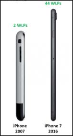
Dick showed an fascinating comparison of the original Apple iPhone which had two WLPs vs the iPhone 7 which had 44 WLPs. One of the 44 is a TSMC InFO-WLP (Integrated Fan-Out) that includes a Package-on-Package (PoP) configuration with the application processor in the bottom package and multiple side-by-side memories in the top package. Apple isn’t the only phone manufacturer using WLP technologies as evidenced by Samsung (Galaxy 7 ; 14 WLPs), Sony (Xperia ; 13 WLPs), Sharp (Aquos Zeta ; 13 WLPs), Huawei (P9 Plus ; 16 WLPs), ZTE (Goophone ; 3 WLPs) etc. On average, there are 15 WLPs per smartphone and the numbers continue to increase.
The shift to WLPs is disruptive on multiple fronts. WLPs remove the need for a laminate substrate which means substrate suppliers are removed from the supply chain. Since WLPs use “wafers” as carriers and traditional thin-film processes for metallization of interconnect, packaging can take place at the foundry as opposed to an outsourced semiconductor assembly and test (OSAT) shop.
Don’t count the OSATs out however. Suresh Jayaraman, of Amkor also presented at the seminar. He gave an overview of Amkor’s Silicon Wafer Integrated Fan-out Technology (SWIFT) offering which is a WLP based on a 300mm wafer carrier. SWIFT uses a “die-last” process that enables processing of the fan-out Redistribution Layers (RDL) in parallel to the die being run in the foundry. This helps Amkor to reduce cycle time once the dice arrive at their shop to be packaged. Suresh also reminded us that they provide a neutral place for die sourced from different foundries to make their way into the same package; remember the need for heterogeneous integration of processors, memory, MEMs, analog, RF etc.
WLP-based SiPs are also disruptive for the CAD tool vendors. Till recently, board and package design were handled by completely different tools than those used for integrated circuits (ICs). SiPs, enabled by WLPs, demand much greater collaboration between board, package and IC designers and a shift to more SiPs could mean new battle lines being drawn between entrenched tool competitors. WLPs also bring many new technical challenges that stress the typical board and package level tools including the advent of very high pin-count packages (> 10,000) and fine-pitch (5um line/space) non-orthogonal routing. With stacking also comes 2D/3D interactions requiring tools to have coordinated views from all three domains (die, package and board).
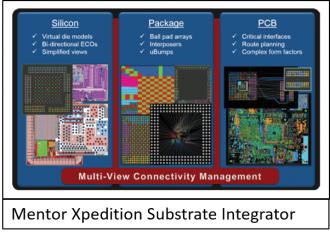
The biggest challenge seems to be the desire to bring data from the disparate domains together to ensure correct connectivity throughout the stack (remember we are now dealing with tens of thousands of signals) and a myriad of new manufacturing design rules from all three domains. To make matters worse, there are almost no standards established between the different domains, let alone the various foundries, OSATs and CAD tool vendors.
Mentor Graphics rounded out the seminar by giving a presentation and live demo of the solutions that they are bringing to the WLP space. The presentation focused on three tools, those being Mentor’s Xpedition Substrate Integrator, Xpedition Package Designer and Calibre 3DSTACK. Xpedition Package Designer focuses on package design and it already includes real-time 2D/3D design viewing and editing. Mentor seems to have this process well in hand.
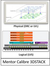
Similarly, the Mentor Calibre team has done a good job of working to bring IC methodologies into the packaging domain by partnering with foundries and OSATs to create what they call an assembly design kit (ADK). The ADK serves much the same purpose as a process design kit (PDK) in the IC world. Using characterized ADKs, Calibre 3DSTACK is able to verify design rule checks (DRCs) and connectivity (LVS) both within the package and across the die / package / board boundaries. Calibre 3DSTACK is also able to do DRC checks on non-orthogonal shapes found on the various RDL layers. The design rules and specifications for these checks are all stored in the ADK.
Mentor’s Xpedition Substrate Integrator tool combines information from all three domains to enable visualization and optimization of complex SiPs by letting designers see the impact of design changes in one domain on the other two domains. This is extremely helpful in an environment where co-design is so essential. The demo given by Mentor was pretty amazing as you could literally see interdependencies of all three domains and trace signal connectivity through the full stack from die pins through various redistribution layers (interposers, WLPs and package), micro-bumps and through-silicon vias (TSVs) all the way to the balls on the ball grid array and finally to the board. It was impressive.
In summary, as systems-in-packages become more prevalent we will continue to see innovation and changes in the both the design and manufacturing eco-systems. Keep an eye out in this area as these changes can and will be disruptive and could cause some shifts in the ecosystems as we know them. Mentor seems well positioned for the new opportunities given their strengths in board, package verification areas.
See also:
Mentor Xpedition IC Packaging Products
Mentor Calibre 3DSTACK


Comments
There are no comments yet.
You must register or log in to view/post comments.