


The transition from FinFET to Gate-All-Around (GAA) transistor technology represents a pivotal moment in the evolution of logic devices, driven by both physical scaling limits and the rapidly growing computational demands of artificial intelligence. As semiconductor technology approaches the sub-3 nm regime, traditional FinFET architectures face fundamental challenges in electrostatic control, performance scalability, and power efficiency. GAA transistors have emerged not as an optional enhancement, but as an essential foundation for sustaining future logic architectures and enabling sustainable AI computing, absolutely.

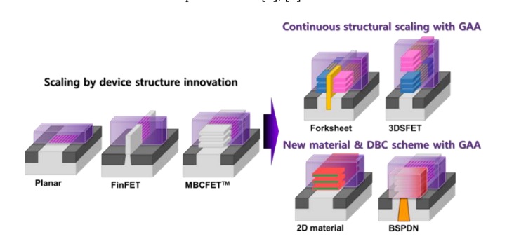
FinFETs were introduced to overcome the shortcomings of planar MOSFETs by improving effective channel width and electrostatic integrity through a three-dimensional fin structure. However, aggressive scaling has exposed inherent limitations in this approach. As fin widths shrink, parasitic resistance increases and carrier mobility degrades due to quantum confinement and surface roughness scattering. Additionally, the three-sided gate configuration of FinFETs struggles to adequately suppress short-channel effects at advanced nodes. These issues collectively constrain further scaling, particularly when standard cell heights approach the ~140–160 nm range.
GAA transistors fundamentally address these challenges by fully surrounding the channel with gate material, delivering superior electrostatic control. This all-around gating enables steeper subthreshold slopes, reduced leakage current, and improved short-channel behavior, even at extremely small dimensions. As a result, GAA architectures re-enable cell height scaling to approximately 100 nm and below, restoring performance and power scaling that had plateaued during the later FinFET generations. This capability has driven industry-wide adoption of GAA as the successor to FinFET technology beyond the 3 nm node.
Beyond electrostatics, GAA devices introduce unprecedented design flexibility. Unlike FinFETs, which rely on discrete fin counts to adjust effective width, GAA transistors allow continuous tuning of nanosheet width. This feature enables designers to finely balance speed and power consumption within the same process node. Wider nanosheets support high-performance computing and server applications, while narrower nanosheets reduce power consumption for mobile and AI-centric workloads. This broad coverage across the speed–power spectrum makes GAA particularly well suited for heterogeneous systems and application-specific optimization.
The rise of generative AI and large language models has further amplified the importance of GAA technology. AI workloads demand exponential growth in compute capability, pushing systems toward petascale and exascale performance levels. At the same time, global data center power consumption is projected to increase dramatically, raising concerns about energy sustainability. GAA transistors directly address this tension by enabling higher performance per watt and supporting increased SRAM density. Higher on-chip memory density reduces off-chip data movement, improving data locality and lowering energy costs associated with high-speed interconnects.
Crucially, GAA also serves as a structural platform for future transistor innovations. Architectures such as Forksheet FETs and three-dimensional stacked FETs (3DSFETs) build directly upon the GAA concept, preserving its electrostatic advantages while enabling further area scaling. When combined with backside power delivery networks, these advanced structures offer improved routing efficiency, reduced voltage drop, and enhanced overall performance. Together, these innovations position GAA as the cornerstone of “beyond-GAA” logic technologies.
Bottom line: The transition to Gate-All-Around technology marks a foundational shift in semiconductor design. GAA is not merely a replacement for FinFETs, but a scalable, flexible, and energy-efficient platform capable of supporting future logic architectures and sustainable AI growth. As device scaling continues to confront physical and power-related constraints, the successful implementation of GAA will determine the industry’s ability to meet the performance, efficiency, and societal demands of next-generation computing.
Also Read:
The 71st International Electron Devices Meeting (IEDM 2025)
DAC – The Chips to Systems Conference 2026
Verification Futures with Bronco AI Agents for DV Debug
Share this post via:


Musk’s Orbital Compute Vision: TERAFAB and the End of the Terrestrial Data Center