Intro
My first exposure to hardware prototyping was at Intel back in 1980 when the iAPX 432 chip-set group decided to build a TTL-based wire-wrap prototype of a 32 bit processor to execute the Ada language. The effort to create the prototype took much longer than expected and was only functional a few months before silicon came back. Fast forward to today where you can take your SOC concept and get it into hardware using an FPGA within a day or so when using a Design For Prototyping (DFP) methodology.
Seminar
Synopsys is hosting this worldwide tour forFPGA Prototypingand inviting engineers to learn more about the best practices of prototyping in hopes of bringing this technology to more SOC projects that want an earlier look at how their hardware and software will really work together. I attended the September 27th seminar in Hillsboro, Oregon not far from where I live.
At the seminar I used a laptop running Red Hat Linux and received a free book: FPGA-Based Prototyping Methodology Manual (FPMM), authored by: Doug Amos (Synopsys), Austin Lesea (Xilinx), Rene Richter (Synopsys)
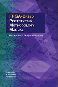
It’s a hefty 470 pages, and was dated February 2011. You can download a free version here.
Our main presenter was Doug Amos, Business Development Manager (SNPS). He has been designing FPGA’s for decades, prototyping for 10 years, and has a British accent.
The seminar sponsors included: National Instruments, Synopsys and Xilinx. The hardware providers all had setups in the back of the room available for us to poke around and look at. It was quite popular and most of us were mesmerized by the blinking lights, cables, buttons and instrumentation.
Synopsys is doing 18 seminar/workshops around the world (Boston, Somerset, Toronto, Austin, Dallas, Mountain View, Irvine, Bellevue, Hillsboro, Paris, Munich, Reading, Hertzliya, Tokyo, Osaka, Beijing, Shanghai, Hsinchu)
The vision is capturing best practices for FPGA-based prototyping, and creating a place where a worldwide group of prototyping professionals can share what they learn.
There’s an online component of the FPMM with a forum, blogs and download of the book. Start the conversation in the seminar, then continue it online.
The Synopsys IP group does FPGA prototyping for their own designs and we had a few of these engineers in the room during our seminar in Hillsboro to ask questions.
Xilinx is the most popular choice for FPGA prototyping because of their high capacity to support SOC designs. The prototyping methodology could be applied to any FPGA vendor, it isn’t specific to Xilinx.
National Instruments was a sponsor, and once the prototype design is in the lab, they can help you to control all of the equipment.
Other book contributors include tier-one design companies: ARM, Freescale Semi, LSI, STMicroelectronics, Synopsys, TI, Xilinx
The book even has a review Council – Nvidia, ST, TI, Broadcom. This makes the book not just a plug for Synopsys but rather an industry attempt at sharing best practices.
Design For Prototyping (DFP) – this was the new three letter acronym that we learned about. In order to get the best prototyping experience you have to alter your design flow.
Gary Gauncher from Tektronix was introduced and later shared about his experience using FPGA prototyping.
Torrie Lewis from the Synopsys IP group that designed PCI Express was introduced to us.
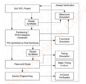
Design Flow for Prototyping
Slides
Keynote – Design-for-Prototyping
Why do we prototype? (the survey results from 1648 users)
[LIST=1]
Verification – did I get what I designed?
Validation – did I get the right thing?
Where can Prototyping help most? (hardwoare bring-up, firmware driver, application sw, code qa and test)
- physical layer
- at speed debug
- regression test (much higher volume of data pushed through)
- multi-core integration
- in-field test
“pre-silicon validation of the embedded software.”, Helena Krupnova, STMicroelectornics
Advantages – find sw bugs
- debug multicore designs
- real time interfaces
- cycle-accurate modeling
- real world speeds
- portable
- low-ccost replication
- uses same RTL as SoC
Challenges to FPGA prototyping (survey size 1649)
[LIST=1]
Best FPGA prototyping – must be an FPGA expert to get the best results
- partition across multiple chips
- hard to achieve silicon speeds
- complicated to debug
- RTL must be available
- RTL not optimized for FPGA
- Considerable setup time required
DFP –methodology to get into FPGA prototype earlier, more reliably
– don’t compromise SoC design goals
How can things be improved? (If you change your SoC design methodology you can get into prototype quicker, saving weeks of time)
- Procedural Guidelines
- Technical Guidelines (FPMM, Chapter 9)
Reuse Methodology Manual (RMM) – co-written by SNPS and MENT, good practice is to avoid latches in SoC (also good for prototyping).
1985 – first FPGA design using Karnaugh map entry.
Advanced FGPA Design today – 5 to 10 million gates possible, RTL, SystemVerilog or C entry
- verification techniques being used
- does simulation do the same thing that my board does?
ASIC design – even when 1[SUP]st[/SUP] silicon comes back you can still use the prototype to help debug silicon
- goal is to use SW the first day that silicon comes out
- does your IP choice exist in FPGA version as well?
System to Silicon tool flow – FPGA based prototyping is a central theme to enable this methodology
Example: HDMI IP prototyped in FPGA
- Xilinx IP, Synopsys IP, new IP under test
- Used a HAPS board with daughter cards for HDMI IO
Technology Update – Bigger, faster prototypes, more quickly
- Stacked silicon interconnect technology (multiple-die stacked together)
- Virtex-7 2000T
- Silicon interposer (metal interconnect between FPGA slices)
- 10K routing connections, ~1ns latency (faster than pins)
- 2 million gates (4 slices of 500K gates)
- More Block RAMS (BRAM)
- Long lines of interconnect, ~1.2ns delays across regions
- About one year before Synopsys has boards using Virtex-7 2000T
FPGA-based Prototyping Flow
- Front end tool (Certify), automated ASIC code conversion and partitioning (about 10 years old)
- Certify outputs to synthesis tool (Synplify Premier)
- Identify, instrument the design, RTL name space used, at speed debug using RTL source
- High Performance ASIC Prototyping (HAPS, Swedish company acquired by Synplicity ), boards or boxes
- Compare Verilog (VCS) versus prototype (using UMRBus) results [FPMM, p336]
Freescale – designing chips for phones, chips must be tested for certification
- tried emulators for certification, protocol test ran in 21 days
- used prototyping for certification using a HAPS 54 board [FPMM, p30], protocol test ran in 1 day
Prototyping – Design and build your own boards, or use HAPS off the shelf?
- cost comparison spreadsheet included
National Instruments – Lab bench has Signal/Pattern generator for stimulus, then scopes for evaluation
- LabVIEW software controls a PXI box for both stimulus and measurements
- Virtual Instruments (VI)
- Create a GUI in LabVIEW to control your designs
Gary Goncher (Tektronix) – User experience with FPGA-based prototyping
- Tektronix Component Solutions, subsidiary of Tektronix, custom chips, package, component test, RF& Microwave modules, data converters
- Designed a high speed data converter board
- TADC-1000 Digitizer Module, 8 bits, 9.5GHz bandwidth, 12.5 GS/s (10 Gibts/s)
- Can we get high-speed data into an FPGA?
- Used a HAPS board to connect their data converter board using a customer daughter board (digitizer interposer board)
- Customers use this setup for multichannel RF receiver, multichannel waveform generator, waveform generator with feedback, RF-in to RF-out system
- Customers can prototype their ideas using this Tektronix / HAPS system, then create their own custom boards
Lab time
I logged into a laptop and went through the lab exercise using Certify and Synplify Premier tools, working on a public-domain processor and getting it through the prototype process in under one hour of time.
Along the way I ran scripts that automated a lot of the time-consuming grunt work to get my RTL in shape for prototyping. I had used Synplify for FPGA synthesis before and so the whole GUI of Certify was familiar to me and the lab work proceeded as documented.
We mapped the processor design across two FPGAs just to get a feel for how partitioned worked.
Most designers should be up and running within a day or so on their designs, it helps to have an experienced AE around to give you a tutorial on the tools.
Photos
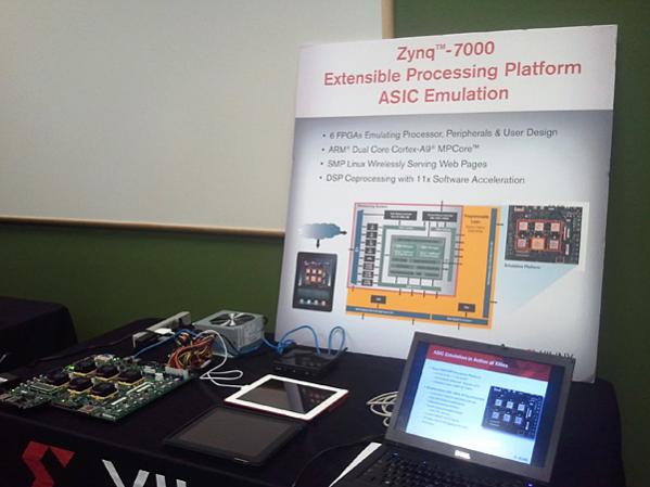
Xilinx Zynq 7000
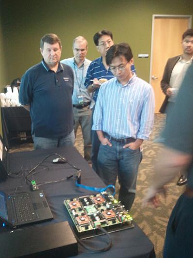
Synopsys IP Group using FPGA Prototype
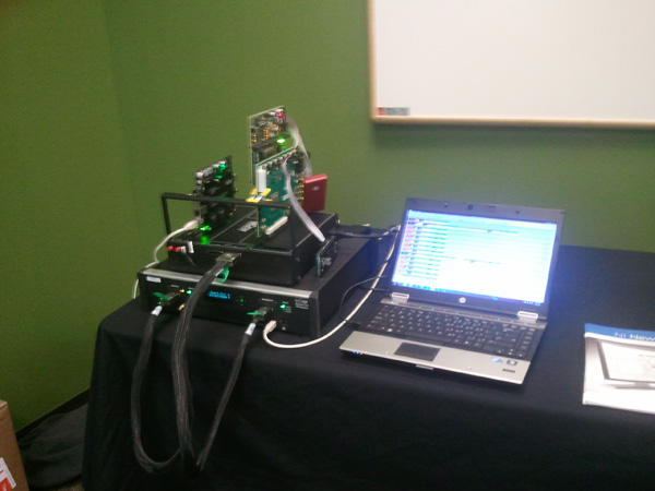
National Instruments setup
Post Lab
Some of the issues for creating a prototype are: SoC design may not be FPGA ready – Pads, BIST, Gate-level netlists, cell instances, memories, clocks, IP
- Automatic Clock Conversion scripts (gated clocks, generated clocks)
- IP with DesignWare, directly use this IP in FPGA prototype
- RTL Input, Partitioned (by Ceritify), synthesis (by Premier), debug (Identify)
Xilinx showed off their ARM Dual Core Coretex-A9 Plus FPGA – ZynqTM
- prototype of an FPGA
Doug Amos – wrap up from Synopsys.
Design-for-prototyping – thinking about prototyping before the spec is complete
Modern Verification Environment – stimulus, DUT, observe
- assertions
- UVM (Universal Verification Methodology)
- Hundreds of functions used to stimulate and verify
- Random stimuli (after functional stimuli), constrained random
- More effort to verify than to design an SoC, even more SW effort than verification effort
RTL for prototyping – maybe change only 1% of your files to make them ready for prototyping (pull out BIST, no pads, remove analog, etc.)
Board-level design has been prototyped – re-verify my functional test bench with my prototype (hardware in the loop), confirm that board behaves as functional simulation (HDL Bridge tool)
Prototypers can influence both SW and HW specifications.
Adopting DFP
[LIST=1]
[LIST=1]
[LIST=1]
Summary
I learned that FPGA Prototyping is a well-understand methodology that can benefit SOC designers that need to get early access to hardware and software running together. The ebook download is filled with practical examples of how to get the most out of your prototyping experience. I recommend the seminar to any designer that wants a solid introduction to the prototyping process.


Comments
There are no comments yet.
You must register or log in to view/post comments.