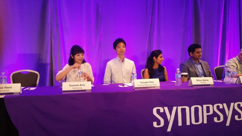
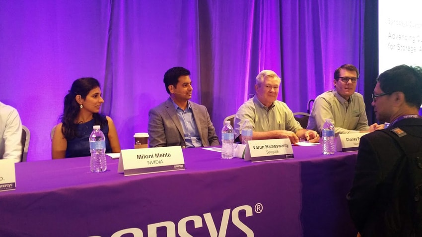
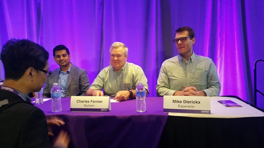
At #55DAC in SFO the first day is always the busiest on the exhibit floor, so Monday by lunch time I was hungry and took a short walk to the Marriott hotel nearby to listen to AMS experts from several companies talk about their EDA tool use, hosted by Synopsys:
- Samsung
- Toshiba Memory Corp.
- NVIDIA
- Seagate
- Numem
- Esperanto
From Synopsys there was Dave Reed who introduced each AMS expert and reminded us that internally at Synopsys they have some 1,400 engineers using the Custom Compiler tools (schematic capture, layout, simulation, extraction, DRC/LVS).

Sunmin Kim from Samsung talked about their foundry design services and AMS challenges like: large number of PVT corners, Monte Carlo run times. For circuit simulation their group uses FineSim, HSPICE and CustomSim, and they automate parts of the analog flow using Tcl scripts. Through a GUI they can setup multiple testbenches, launch Monte Carlo runs over PVT corners, perform circuit checks, determine if circuits are passing or failing, use a results viewer for data mining, and review reports generated.
Circuit designers can use the calculator to measure results and compare against the specifications, compare the results of Monte Carlo simulations, look at eye diagrams and even perform stability analysis. In the GUI the passing simulation results will show up in green, while failures display in red, so you can pinpoint what to tweak in order to meet specs.
Next up was Yusuke Ono from Toshiba Memory Corp where they design flash memory chips. FineSim is used for circuit simulation of 3D flash memory. For highest integration they use a 3D stacking approach, reaching some 64 layers in 2017 and 96 layers by the end of 2018. Their biggest engineering challenges are simulation capacity, speed, accuracy and handling multiple power domains.
They first started using FineSim back in 2004 as a sign-off circuit simulator, and they also do IR drop and EM analysis as well. There’s a useful parameter in FineSim called finesim_flash, where setting it to 1 provides highest accuracy, and using 2 for fastest speed, allowing the designer to make a trade-off. The 2 value can show up to 2.8X faster simulation times.
NVIDIA sent Miloni Mehta to present their design of GPU chips, and one of their challenges was to do full-chip self-heat prediction using machine learning. GPU chips power computing for an ever-widening list of applications, like: computer gaming, graphics, AI, healthcare, retail, robotics and self-driving cars.
As a GPU is powered up it begins to generate self-heating which in turn causes a Vt shift and requires Electro-Migration reliability issues. Using a circuit simulator like HSPICE you can do self-heating simulations, but that process can be time consuming and typically is only used on smaller cells, so how do you find which cells require self-heating simulations?
The answer was to use machine learning to identify which cells require self-heating simulations. To do this they started out with PrimeTime to find cells along paths, then generated a ML model with Tensor Flow. They validated the ML model to confirm results. The model predicts self-heating effects then they check for any errors by using HSPICE measurements. A deep neural network (DNN) was used for ML, although they did try a few other methods but DNN captured all of the non-linear relationships the best. For their DNN there was one input layer, three hidden layers and the output predicts self-heating based on sampled data.
Some of the challenges faces with this project were obtaining the accuracy required at higher temperatures, finding the best learning algorithm, and not overfitting the data. For training they used 6,000 cells and then for validation they used 2,000 cells. Their ML approach was able to show capacitive loading versus temperature, frequency versus temperature, cell size versus temperature, and resistance versus temperature.
The results of using ML showed a good correlation between predicted self-heating and simulated self-heating using HPSICE, so that they could then filter out 99% of the cells from needing HSPICE for self-heating simulations, way more efficient than brute-force HSPICE self-heating on all cells.

Varun Ramaswarmy from Seagate told us how his company does HDD and SSD products with some 41,000 employees. They had a goal to do a new SoC tapeout in just 12 months using an improved CAD tool flow with rapid PDK deployment, using automation for improved productivity, and having a similar workflow to Virtuoso on the front-end. At first their mask designers were hesitant to change from Virtuoso to Custom Compiler, but with close collaboration with Synopsys, they created a flow that met all their needs.
The GUI-based revision control system worked well for the team and the analog tool flow had: schematic capture, test bench creation, circuit simulation using HSPICE and FineSim, DRC/LVS checks, parasitic extractions, and finally fully extracted circuit simulations.
On the PLL block they used AFS for circuit simulation, IC Validator instead of Calibre, and also used the CustomSim simulator. Their tool flow with Custom Compiler was more productive compared to using Virtuoso:
- 10% faster PDK
- 5% faster front-end
- 15% faster mixed-signal verification
- 15% faster back-end
- 20% faster physical verification

Numem is doing MRAM designs and Charles Farmer shared their ambitious plans to reach tape-out in just 3 months using a 22nm process to create a working 20Mb MRAM. Their team used an all Synopsys tool flow: Custom Compiler, IC Validator, StarRC, HSPICE, CustomSim, FineSim, VCS. The sense amp design was simulated with FineSim for highest accuracy, and FineSim Pro was used on digital logic cells for highest speed. Schematic-driven layout was used, and for mixed-signal simulation they used VCS and CustomSim. Design and version management was handled by the ClioSoft tool. With a one-vendor flow there was no finger-pointing between EDA vendors, and support was excellent.
Our final speaker during the luncheon was Mek Dierickx from Esperanto Technologies, a start-up doing a machine learning processor chip. To reach ultimate energy efficiency they chose a two-core approach with a RISC-V architecture, including a memory that is specific to ML. They wanted to solve two big problems: power scaling and frequency scaling, while taking on the challenges of a 7nm process node.
Mask designers used SDL (Schematic-driven Layout), symbolic editing and design-rule driving layout where you avoid having to use rulers to make measurements all of the time. Custom Compiler and IC Compiler II are pretty seamless to use, because you can open an ICC2 file in CC, or open a CC file in ICC2, just pick the right tool for the editing job at hand.
Their team was able to design and layout 55 leaf cells in just 4 months using Custom Compiler, about 2X faster than a Virtuoso flow. With the CC+ICC combination they were able to finish their tasks about 10X faster with ECO turns done in a day. As a result they could complete their new ML processor design which much fewer mask designers and circuit designers than when using previous flows.
Summary
All of the speakers stayed at the platform to handle questions from attendees and this luncheon event really let the CAD folks and tool users talk about their good experiences using Synopsys tools for analog and mixed-signal design challenges spanning the gamut from billion-transistor GPU designs down to small libraries of cells. There certainly was a buzz at DAC this year on all things AI, ML and neural networks, so these speakers hit on all of those segments.
It looks like Synopsys has done a decent job of integrating all of their point tool acquisitions over the past years (Springsoft, Ciranova, Magma, Nassda) into a cohesive tool flow for custom IC design, and I expect that competition is healthy for our industry because it forces the EDA vendors to continually invest in automation.
Watch the complete video of the luncheon speakers.
Related Blogs
Share this post via:


Comments
There are no comments yet.
You must register or log in to view/post comments.