Every SoC project that I know of wants to finish on time, under budget, and maximize profits per device. When I first started out doing DRAM design I learned that we could maximize profit by doing shrinks of existing designs, move from ceramic to plastic packages, and reduce the amount of time spent on a tester. Today, the economic reality is similar, and so this blog is focused on saving tester time which directly impacts product costs. My source for the latest info on reducing test costs came from both Advantest in the ATE (Automatic Test Equipment) world and Synopsys in the DFT (Design For Test) software segment as part of a webinar given last month, and now archived. Divide, parallelize and test is a proven cost-reduction approach for both multisite test with multiple devices and concurrent test with multiple IP blocks within the SoC.
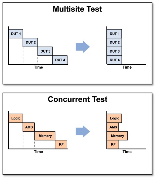
We often blog about how beneficial it is for collaboration between EDA, IP and Foundries to ensure design success, but there is also collaboration going on between ATE and EDA to ensure better test results and higher profits through lowered tester times.
Related – Two New Announcements at ITC from Synopsys
Multisite Test
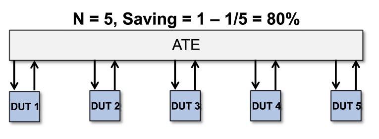
Adam Cron from Synopsys showed that every ATE system has a limited number of channels, so the greatest multisite count is: # ATE Channels / # Pins per die. The equation for percentage time saving with multisite is then: 1 – 1/N. As an example with N=5 the maximum time savings are 80%:
With stimuli broadcast all of the inputs to the DUTs receive the same data, so you can test more devices with fewer ATE channels:
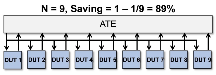
Factors that increase the multisite test time were discussed: edge dies, test resources, index time and branching during test flow.
Related – Catching IC Manufacturing Defects with Slack-Based Transition Delay Testing
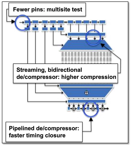
The DFT software from Synopsys that supports multisite and concurrent test is called DFTMAX Ultra and it features:
- Hardware test compression for data reduction
- Simplified scan shift clocking
- Uses fewer pins, down to 1 SI (Scan In) and 1 SO (Scan Out)
- Power-aware during scan testing to stay in spec
- Synthesis-based to minimize iterations between design and test
Concurrent Test
Dave Armstrong from Advantest was up next in the webinar and talked about how their company is #1 in ATE, and that their two most popular testers are the V93000 and T2000 models.
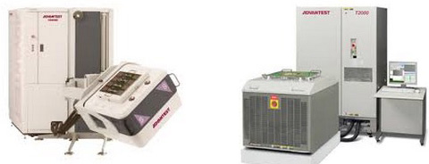
Advantest V93000 and T2000 testers
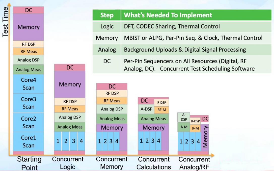
These ATE systems have from 8K to 12K pins and can support a pattern depth of 32 Gbit. As a conceptual example of concurrent test a four core SoC with multiple IP blocks was considered, showing how you could start out with a purely sequential test approach, then gradually refine to add more parallelism thus decreasing test time.
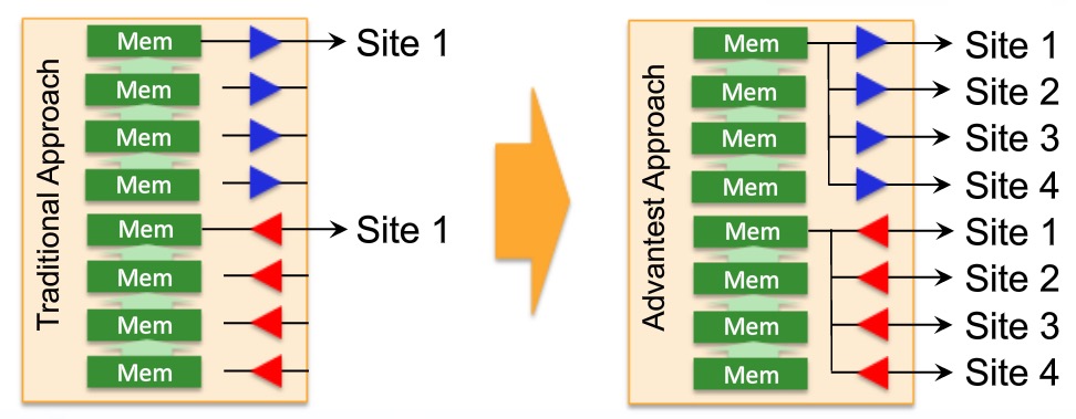
An approach called memory pooling allows you to add ATE channels together adding more depth to 32 Gbit in the most efficient manner.
Branching in a test flow is often used for binning based on performance, so the Advantest approach is to parallelize the multiple branch paths.

Both multisite and concurrent approaches help reduce test times and require:
- High pin-count ATE with flexibility
- DFT tools with hardware compression
- A fast-responding thermal control environment
Summary
EDA and ATE companies are collaborating to drive down test time through hardware compression, DFT tools and methodologies. Synospys and Advantest have shown how that you can save time and money on your next SoC project by using concurrent and multisite test techniques.
- Full webinar online, about 35 minutes in length.


Comments
0 Replies to “Saving Time and Money on Your Next SoC Project”
You must register or log in to view/post comments.