You are currently viewing SemiWiki as a guest which gives you limited access to the site. To view blog comments and experience other SemiWiki features you must be a registered member. Registration is fast, simple, and absolutely free so please,
join our community today!
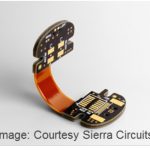
I first met John Durbetaki at Intel in Aloha, Oregon and we both had a keen interest in the nascent personal computer industry. My first PC was made by Radio Shack and dubbed the TRS-80 which maxed out at 48KB of RAM. I kept watch on Durbetaki as he left Intel and formed his own company OrCAD in 1985 to serve the needs of PC-based CAD software.… Read More
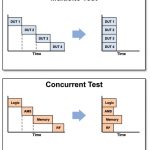
Every SoC project that I know of wants to finish on time, under budget, and maximize profits per device. When I first started out doing DRAM design I learned that we could maximize profit by doing shrinks of existing designs, move from ceramic to plastic packages, and reduce the amount of time spent on a tester. Today, the economic … Read More
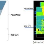
It feels to be at the top of semiconductor technology by having dies with high density of semiconductor design at sub-20nm technology node stacked together into a 3D-IC to form a complete SoC which can accommodate billions of gates. However there are multiple factors to be looked at in order to make that successful amid often conflicting… Read More