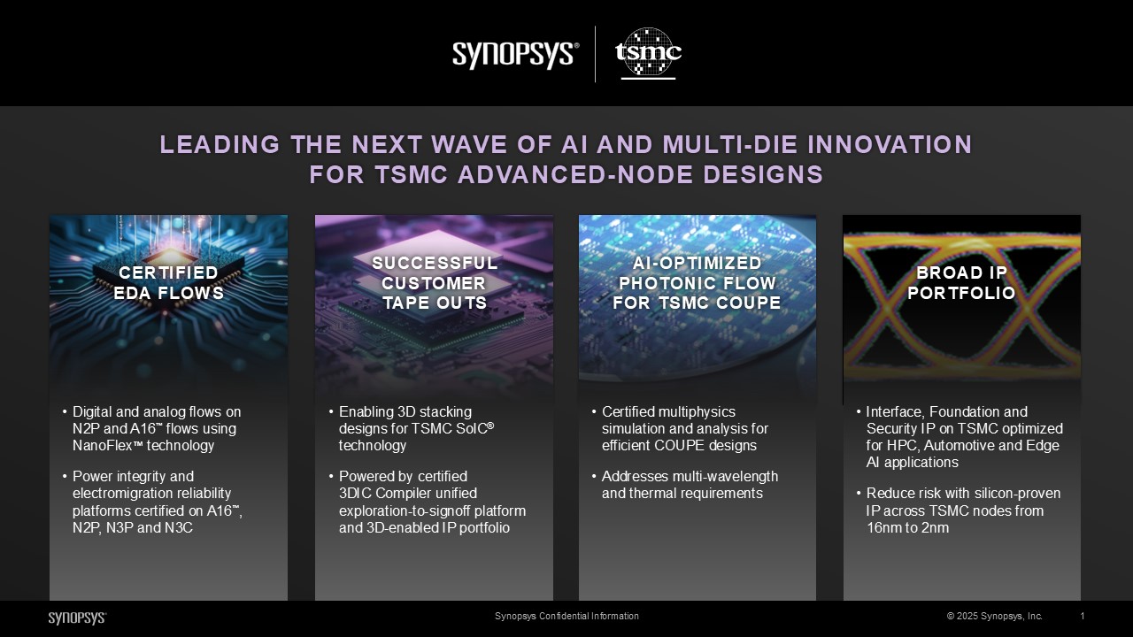
Synopsys has deepened its collaboration with TSMC certifying the Ansys portfolio of simulation and analysis tools for TSMC’s cutting-edge manufacturing processes including N3C, N3P, N2P, and A16. This partnership empowers chip designers to perform precise final checks on designs, targeting applications in AI acceleration, high-speed communications, and advanced computing. Additionally, the companies have developed an AI-assisted design flow for TSMC’s Compact Universal Photonic Engine (COUPE™) platform, streamlining photonic design and enhancing efficiency.
Multiphysics and AI-Driven Design Innovations
Synopsys and TSMC are advancing multiphysics analysis for complex, hierarchical 3DIC designs. The multiphysics flow integrates tools like Ansys RedHawk-SC™, Ansys RedHawk-SC Electrothermal™, and Synopsys 3DIC Compiler™ to enable thermal-aware and voltage-aware timing analysis. This approach accelerates convergence for large-scale 3DIC designs, addressing challenges in thermal management and signal integrity critical for high-performance chips.
For TSMC’s COUPE platform, Synopsys leverages AI-driven tools like Ansys optiSLang® and Ansys Zemax OpticStudio® to optimize optical coupling systems. These tools, combined with Ansys Lumerical FDTD™ for photonic inverse design, allow engineers to create custom components, suhttps://www.ansys.com/products/connect/ansys-optislangch as grating couplers, while reducing design cycle times and improving design quality through sensitivity analysis. This AI-assisted workflow is transformative for photonic applications, enabling faster development of high-speed communication interfaces.
Certifications for Advanced Process Technologies
The collaboration includes certifications for key Synopsys tools across TSMC’s advanced nodes. Ansys RedHawk-SC and Ansys Totem™ are certified for power integrity verification on TSMC’s N3C, N3P, N2P, and A16™ processes, ensuring reliable chip performance. Ansys HFSS-IC Pro™, designed for electromagnetic modeling, is certified for TSMC’s N5 and N3P processes, supporting system-on-chip electromagnetic extraction. These certifications enable designers to meet stringent requirements for AI, high-performance computing (HPC), 5G/6G, and automotive electronics.
Additionally, Ansys PathFinder-SC™ is certified for TSMC’s N2P process, offering electrostatic discharge current density (ESD CD) and point-to-point (P2P) checking. This tool enhances chip resilience against electrical overstress, accelerating early-stage design validation and improving product durability, particularly for complex 3DIC and multi-die systems. Synopsys is also working with TSMC to develop a photonic design kit for the A14 process, expected in late 2025, further expanding support for photonic applications.
Industry Impact and Strategic Partnership
This collaboration underscores Synopsys’ leadership in providing design solutions for next-generation technologies.
“Synopsys provides a broad range of design solutions to help semiconductor and system designers tackle the most advanced and innovative products for AI enablement, data center, telecommunications, and more,” said John Lee, vice president and general manager of the semiconductor, electronics, and optics business unit at Synopsys. “Our strong and continuous partnership with TSMC has been a key factor in maintaining our position at the forefront of technology while providing consistent value to our shared customers.”
“TSMC’s advanced process, photonics, and packaging innovations are accelerating the development of high-speed communication interfaces and multi-die chips that are essential for high-performance, energy-efficient AI systems,” said Aveek Sarkar, director of the ecosystem and alliance management division at TSMC. “Our collaboration with OIP ecosystem partners such as Synopsys has delivered an advanced thermal, power and signal integrity analysis flow, along with an AI-driven photonics optimization solution for the next generation of designs.”
Bottom line: By combining Synopsys’ simulation expertise with TSMC’s advanced process technologies this partnership accelerates the development of robust, high-performance chips, solidifying both companies’ roles in shaping the future of semiconductor design, absolutely.
The full press release is here.
About Synopsys
Synopsys, Inc. (Nasdaq: SNPS) is the leader in engineering solutions from silicon to systems, enabling customers to rapidly innovate AI-powered products. We deliver industry-leading silicon design, IP, simulation and analysis solutions, and design services. We partner closely with our customers across a wide range of industries to maximize their R&D capability and productivity, powering innovation today that ignites the ingenuity of tomorrow. Learn more at www.synopsys.com.
Also Read:
Synopsys Announces Expanding AI Capabilities and EDA AI Leadership
The Rise, Fall, and Rebirth of In-Circuit Emulation (Part 1 of 2)
448G: Ready or not, here it comes!
Share this post via:


Comments
There are no comments yet.
You must register or log in to view/post comments.