Multi-die design has become the center of a lot of conversation lately. The ability to integrate multiple heterogeneous devices into a single package has changed the semiconductor landscape, permanently. This technology has opened a path for continued Moore’s Law scaling at the system level. What comes next will truly be exciting. Before getting too excited it’s important to realize there are still substantial challenges presented by this new method of system design.
These challenges are interrelated and span from architectural all the way to manufacturing and deployment in the field. Solving these problems is a multi-dimensional balancing act. A holistic approach is the only effective strategy. The problem is actually broader than multi-die design. It also includes new communication strategies, new materials, new thermal and mechanical problems among others. The term heterogeneous integration is more accurate. There are few companies with the breadth and depth of capability to tackle this class of problem. Synopsys is one of those companies and they have taken a unique approach. I examined some aspects of the Synopsys solution in a recent post. Let’s go deeper and examine what is different about Synopsys’ comprehensive, scalable solution for fast heterogeneous integration.
Early Architecture
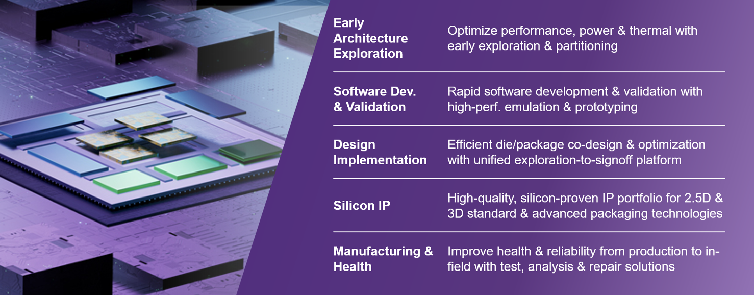
The graphic at the top of this post presents a good overview of the multi-dimensional nature of heterogeneous integration. It turns out Synopsys has published a series of white papers that cover the full spectrum of the problem. Taken together, this material presents all the elements of a master class on the topic. I highly recommend taking the time to read them all. Links are coming. Let’s first take a quick look at what each white paper offers. I’ll start with the early architecture topics.
This first white paper begins with an overview of the various tasks that must be considered to achieve a successful multi-die design project. Those items are summarized in the figure below.
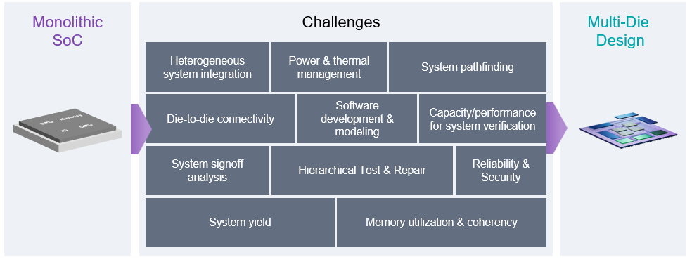
This white paper focuses on system pathfinding, memory utilization & coherency, and power/thermal management. A key to successful multi-die design is a virtual prototyping environment for early architecture exploration. This environment allows architects to capture the hardware resources of their multi-die design. The architecture of such a system is described.
Key items that are analyzed and balanced here include workload and architecture definition, partitioning and technology selection, and early performance and power analysis. The Synopsys Platform Architect for Multi-Die is described, which addresses all these requirements and more.
System Verification and Validation
The next white paper discusses the challenges of verification and validation for multi-die designs. Areas of focus here include addressing capacity and performance for system verification, validating assumptions made during architecture design, and knowing when verification is complete. Simulation and emulation models must be able to scale with the design size and make best use of the available resources. It is also important to consider analog components, which must either be modeled digitally or co-simulated in a mixed-signal environment.
The white paper goes on to point out that the key to addressing the challenges outlined above is recognizing that a multi-die design is not a single design, but rather a combination of independently manufactured designs (dies) interconnected through communication fabrics. The figure below provides a disaggregation example, showing how a monolithic design becomes a combination of dies, creating numerous verification challenges.
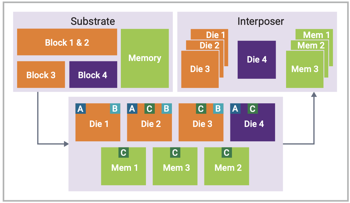
It is explained that, to perform system-level tests, the RTL designs for all the dies must be assembled and simulated in a single executable. This presents many challenges, including:
- How can “independent” designs and testbenches be assembled into one simulation environment?
- Can the die-level testbenches be reused or synchronized?
- Does the compute server have enough memory to build and execute the simulation?
- Can the simulation be distributed over multiple servers?
- How can name clashes be avoided?
The paper goes on to describe the Synopsys VCS® functional verification solution, that provides a powerful and flexible approach to multi-die design simulation. Details of how NVIDIA used this capability on a real design are also provided.
Design Implementation and Signoff
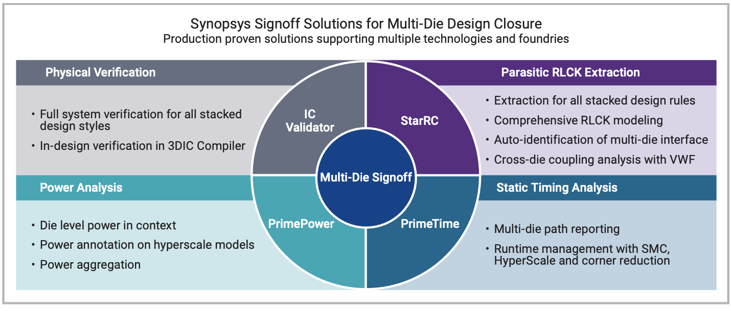
Next, we examine the challenges of implementation and signoff. This white paper discusses the challenges faced here, which include signoff for multi-die extraction and timing, multi-die power, and multi-die physical design.
The white paper explains that multi-die signoff is impossible with traditional 2D timing, checking, and power analysis tools. For example, signals that cross between dies pass through multiple stacked layers, including interposers and substrates, and the delays through these layers must be considered for static timing analysis. This places new requirements on both physical verification and parasitic extraction.
In addition, power calculations are more complex since they must combine the results for all dies. Multi-die design also requires innovation for design rule checking (DRC), layout versus schematic (LVS) verification, and other physical checks. The reality is that accurate multi-die signoff requires the entire stack to be considered in a holistic way.
The paper describes the suite of tools Synopsys provides to address these challenges in an integrated and unified way. The figure below summarizes the technologies discussed.
Silicon IP Integration
This white paper examines the challenges of efficient multi-die design implementation and IP integration. UCIe, as a specification for die-to-die interconnect is discussed. The complexities of a multi-die package with UCIe expressing die-to-die connectivity are reviewed.
An example shows one UCIe link on the I/O chiplet (Die 1) being connected through the package with the other UCIe link on the CPU/compute die (Die 2). The UCIe link consists of a physical layer (PHY) and a controller. The UCIe PHY includes the transmit/receive (TX/ RX) pins, which must be routed through the package to the UCIe PHY on the other die. The UCIe PHY IP is composed of 8 DWORDs, is placed in a row next to each other. Each DWORD consists of a pair of clocks, 64 single-ended data lanes, a data valid lane in each direction (transmit and receive), and a track lane. Additionally, there is a low-speed sideband bus for initialization, link training, and configuration read writes.
The diagram below illustrates this configuration.
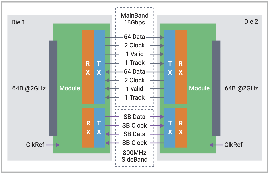
This white paper goes into the details of how the combination of Synopsys UCIe IP and Synopsys 3DIC Compiler enable higher productivity with lower IP integration risk by automating routing, interposer studies, and signal integrity analysis. There’s a lot to consider here, both in terms of IP choices for communication and implementation of complex interconnect schemes. You will get a good appreciation of the completeness of the Synopsys solution.
Manufacturing and Device Health
The final white paper discusses effective monitoring, test, and repair of multi-die designs. The piece points out that multi-die designs are more costly to build and test than traditional single-die packages. Only one failed die in a multi-die configuration can cause the entire system to fail. Thus, the quality of each die and the integrity of the interconnect is critical.
This white paper goes into significant detail regarding the array of Synopsys solutions to cover test, repair and device health through its lifetime. It also explains how Synopsys IP is integrated into the chip design to implement these capabilities.
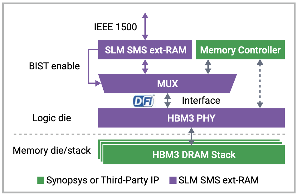
HBM is a popular standard for integrated memory in multi-die designs. The standard defines an interface for 3D-stacked synchronous dynamic random-access memory (DRAM) dies. It specifies the PHY-level logic-to-memory interconnection. The white paper describes how Synopsys SLM SMS ext-RAM IP supports at-speed interconnect test and diagnosis of memory dies as well as post package repair (PPR).
This IP provides:
- Comprehensive at-speed interface and memory array testing and diagnosis
- Programmable test algorithms, address types and ranges, test operation time, and DRAM access timing
- Diagnostics data reporting
- Memory fault type and failing address/data lanes
- Post-packaging repair via HBM stack repair signature
The figure below shows how the pieces fit together.
To Learn More
This is just a high-level summary of the broad coverage Synopsys offers for multi-die design and heterogeneous integration. The white papers mentioned provide substantially more detail. If a multi-die design is in your future, you will find this material to be quite valuable. Here is where you can get your own copies:
Early Architecture Performance and Power Analysis of Multi-Die Systems
Overcoming the Challenges of Verifying Multi-Die Systems
Achieving Successful Timing, Power, and Physical Signoff for Multi-Die Designs
Enabling Efficient Multi-Die Design Implementation and IP Integration
Effective Monitoring, Test, and Repair of Multi-Die Designs
This information will help you better understand what is different about Synopsys’ comprehensive, scalable solution for fast heterogeneous integration.
Also Read:
Will 50% of New High Performance Computing (HPC) Chip Designs be Multi-Die in 2025?
A Deep Dive into SoC Performance Analysis: What, Why, and How
Share this post via:


Comments
There are no comments yet.
You must register or log in to view/post comments.