This is another installment covering TSMC’s very popular Open Innovation Platform event (OIP), held on August 25. This event presents a diverse and high-impact series of presentations describing how TSMC’s vast ecosystem collaborates with each other and with TSMC. The presentation covered here from Synopsys focuses on the unique needs of training and inference for AI/ML engines. The algorithms implemented by these designs have very specific requirements. Meeting those requirements demands specialized IP. These special needs and the optimized Synopsys DesignWare IP are discussed to illustrate how AI/ML SoCs get a boost from Synopsys IP on TSMC’s 7nm and 5nm processes.
The presentation was given by Faisal Goriawalla, senior product marketing manager at Synopsys. Faisal has over 18 years of engineering and marketing experience in embedded physical IP libraries and non-volatile RAM. He started his career developing embedded SRAM memory compilers and before Synopsys held various technical and marketing positions for memories, standard cells and I/O libraries at ARM. Faisal’s strong background inspires confidence.
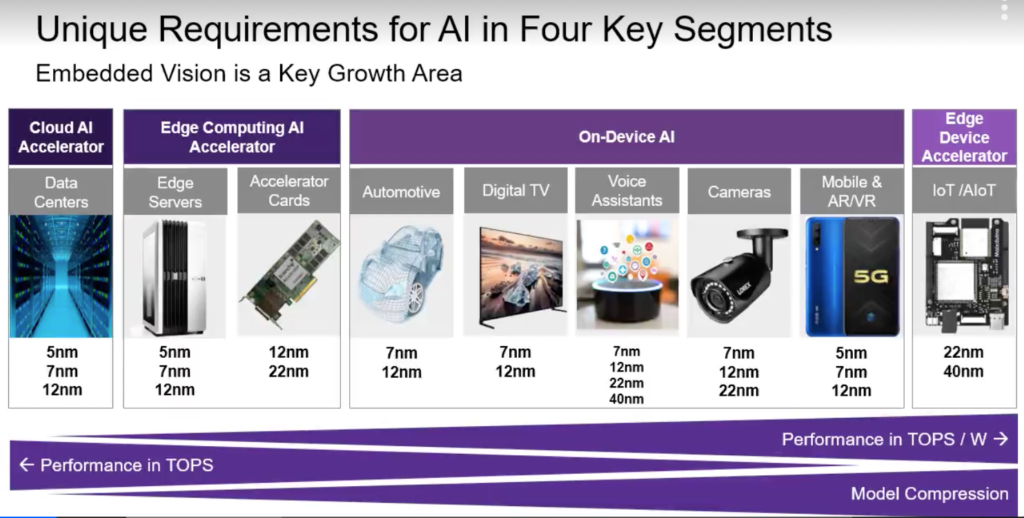
Faisal began his presentation focusing on the unique requirements of deep learning and convolutional neural networks (CNNs). He explained that CNNs create a mathematical graph of a problem and train it with a data set of known values. The process begins with training the network, which is compute intensive and then proceeds to inference, where the trained model is deployed. He went into a very good explanation of the requirements of various AI problems with regard to performance, model compression and power. The diagram below summarizes this discussion.

He then explained some of the aspects of a CNN and how it is used to process two-dimensional data. This segment of the presentation provides a very good overview of AI algorithms. I recommend watching it if this is of interest.
Faisal then discussed some of the design challenges for AI chips. Of course, power and area are key items, along with a predictable schedule. He pointed out that an application-aware approach is needed to meet these goals. Some of the items to consider with an approach like this include:
- Choosing the right mix of VTs-Lg-tracks
- Converging on an optimal floorplan
- Managing congestion in multiply-accumulate blocks (MACs)
- Navigating the RTL to GDSII flow
- Achieving PPA targets
Faisal went into some detail on these points. The discussion then turned to application-aware IP, what is needed, and what the benefits will be. From an IP component point of view, what is needed to achieve PPA targets includes:
- Low power memories, especially for Read
- Low power combo cells to reduce internal energy
- Complex combinational cells to reduce switching power
- Special clock gates with lower internal power
- Granular delay cells to reduce the area and power cost of hold fix
- Multi-bit flops to reduce active power
From a methodology point of view, what is needed includes:
- Choice of VT-Lg to give a good starting point on PPA
- Power recovery post-route to reduce leakage
- Flow stage correlation never adds >10% to any metric
Faisal then discussed some of the DesignWare IP solutions from Synopsys to address these requirements:
HPC Kit Enhanced for AI Applications
This package includes IP for object detection and recognition. There are special cells to reduce CNN power consumption up to 39%. Tradeoff tuning enables a 7% frequency boost with 28% lower power. The figure below summarizes some of the benefits of the HPC Kit. This IP is typically used for ADAS applications.

Memory Architectures
The benefits of customizing memory architectures to optimize PPA for AI designs was also discussed. Synopsys offers a wide range of architectures, bitcells, VTs and PVTs here, including:
- Ultra-high density, high density and high speed
- Small (128Kb) range register file
- Large (>1Mb) range SRAM
- UHD 2-port memories provide FIFO functionality with smaller area & lower leakage at slower speeds
- Configurable multi-port memories
GPIO Libraries
AI designs are typically core limited (as opposed to pad limited). Inline I/O libraries with a less height and more width form factor are optimal to reduce SoC area for this situation. Synopsys offers DesignWare IO Libraries with:
- High (up to 250MHz) performance and high drive strengths for additional margin while supporting longer trace lengths
- Support for 1.8V, 2.5V and 3.3V I/O supplies (technology dependent) for other interfaces on an AI/ML SoC
DFT
The ability to integrate an on-chip test and repair engine is important for reducing area and power in AI applications. The Synopsys STAR Memory System provides this support. Total core area can be reduced by ~7% and dynamic power can be reduced by ~12%.
Conclusion
Faisal concluded by explaining that the IP discussed is silicon-proven in volume at TSMC 7nm and test silicon proven at TSMC 5nm. You can learn more about Synopsys DesignWare IP for AI here. You can access the TSMC OIP presentations here. AI/ML SoCs truly get a boost from Synopsys IP on TSMC’s 7nm and 5nm.
Also Read:
Parallel-Based PHY IP for Die-to-Die Connectivity
Making Full Memory IP Robust During Design
Share this post via:


Comments
There are no comments yet.
You must register or log in to view/post comments.