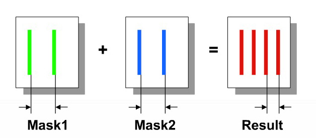
You can’t have failed to notice that 20nm is coming. There are a huge number of things that are different about 20nm from 28nm, but far and away the biggest is the need for double patterning. You probably know what this is by now, but just in case, here is a quick summary.
Lithography is done using 193nm light. Today we use immersion lithography (so instead of the gap between the wafer and the last lens being an air gap it is water). Amazingly, when you think of what you learned in high-school physics (young’s slits, diffraction gratings, never mind anything you might have learned about quantum mechanics) this worked down to 28nm and we could print the features needed with light with 6 times the wavelength. But at 20nm it doesn’t work any more.

Double patterning requires two masks. There are variations on the approach but for 20nm (probably not true for future generations) we split the polygons on the mask into two sets (this is known as coloring since that is what graph-theorists call this sort of thing). Each mask goes through a lithography cycle and we end up with photoresist that has been exposed to both masks. The reason we can just use one mask is that diffraction effects on that one mask would mean the exposure wouldn’t work. It is a light problem, not a problem of manufacturing what gets exposed.
So the new step is separating the polygons on the masks into two groups that are all double the minimum pitch. If you think of a bus just running parallel signals across the chip, then the odd ones go on one mask and the even on the other. But in more complex cases this may not work. It is simple to think up cases where A has to be on a different mask from B (because they are too close) and B has to be on a different mask from C, but that polygon C also goes close to A so it has to be on a different mask from A. Impossible (or we use triple patterning but that is not economic although we will get there if EUV doesn’t work effectively).
But there is another problem. The two masks are not self-aligning (there are self-aligning approaches which will be needed in the future, but for now it looks like most double patterning will be the simpler, aka cheaper, approach). So sidewall capacitance between two adjacent polygons will be much more variable than before depending on whether the masks are at the maximum allowed misalignment in one direction, versus the other direction, versus ‘typical’ meaning perfectly aligned. So a verification methodology that is color aware is needed to get useful parasitic information that can be used to close the design (timing, power, signal integrity, reliability and so on are all affected by this variability).
Synopsys has been working with TSMC and there was webinar presented by both companies to go into the details. The presenters are Anderson Chiu of TSMC and Beifang Qiu from Synopsys. Anderson is the program owner of the TSMC 20nm reference flow (I bet he gets lots of calls from EDA marketing folks). Beifang is the senior R&D manager for StarRC extraction.
Since both presenters are Chinese the webinar was presented not only in English but also in traditional and simplified Mandarin (the difference is in the slides not the language). I’m assuming that all 3 versions of the webinar will be online soon. The Synopsys home page for the webinar still links back to the registration. And if you are interested in that kind of thing, Synopsys and TSMC have a joint press release about the methodology here.
Share this post via:


Comments
0 Replies to “Double Patterning Verification”
You must register or log in to view/post comments.