By Mark Tawfik
Parasitic extraction is essential in integrated circuit (IC) design, as it identifies unintended resistances, capacitances, and inductances that can impact circuit performance. These parasitic elements arise from the layout and interconnects of the circuit and can affect signal integrity, power consumption, and timing. As IC designs shrink to smaller nodes, parasitic effects become more pronounced, making accurate extraction crucial for ensuring design reliability. By modeling these effects, designers can adjust their circuits to maintain performance, avoid issues like signal delays or power loss, and achieve successful design closure.
What is parasitic extraction
In semiconductor design, parasitic elements—like resistances, capacitances, and inductances—are unintended but inevitable components that emerge during the physical fabrication of integrated circuits (ICs). These elements are a result of the materials used and the complexity of the fabrication process. Although not part of the original design, parasitic elements can significantly impact circuit performance. For example, parasitic resistances can cause voltage drops and increased power dissipation, while parasitic capacitances can lead to signal delays, distortions, and crosstalk between adjacent wires. Additionally, interconnect parasitic introduce propagation delays that can affect the timing and signal integrity, leading to higher power consumption and reduced overall performance.
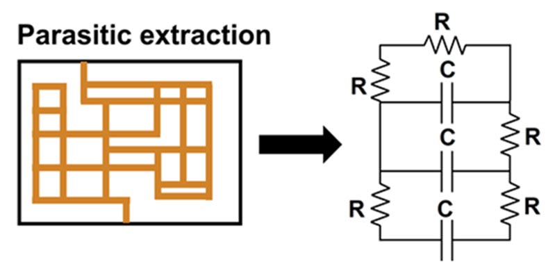
Parasitic extraction is a critical process in IC design that identifies and models these unintended parasitic effects to ensure reliable performance. In digital design, parasitic extraction relies heavily on standardized formats like LEF (Library Exchange Format) and DEF (Design Exchange Format), which describe both the logical and physical aspects of the design (figure 1).

The parasitic extraction process typically follows these key steps:
- Data preparation: This step involves assembling and aligning the logical and physical design data, usually sourced from LEF and DEF files. The purpose is to ensure each logical component is correctly mapped to its corresponding physical location in the layout, ensuring accurate connectivity for the parasitic extraction process.
- Extraction: During extraction, parasitic components such as resistances, capacitances, and interconnects are identified and captured from the design layout and technology data. This forms the basis for understanding how these parasitic elements might impact the overall performance of the circuit.
- Reduction: Once parasitic elements are extracted, they are simplified using models such as distributed RC or lumped element models. These models condense the parasitic data, making it easier to manage while still accurately reflecting the parasitic effects for simulation and analysis.
- Verification: After extraction, the data is subjected to verification. This involves comparing the parasitic data with design specifications and simulation results to ensure it aligns with the expected circuit performance and complies with necessary design rules and criteria for sign-off.
- Optimization: After verifying the parasitics, designers can apply various optimization techniques to reduce their negative impact on the circuit. This can include refining routing paths, adding buffers, or making other adjustments to improve performance, timing, power consumption, and signal integrity.
Accurate parasitic extraction is crucial for successful IC design, particularly as technology advances and parasitic effects become more pronounced. By systematically modeling, verifying, and optimizing these effects, designers can ensure that their circuits perform reliably and meet required specifications during fabrication and final production.
Analog and digital design flows
Analog and digital design flows are two distinct approaches in semiconductor design, each suited to the specific requirements of analog and digital integrated circuits (ICs). Analog design deals with circuits that process continuous signals, such as amplifiers, filters, and analog-to-digital converters (ADCs). Precision is crucial in these circuits to minimize noise, distortion, and power consumption. Designers face challenges like balancing trade-offs between power efficiency and noise reduction, requiring manual layout adjustments to avoid performance issues caused by small variations. Tools like SPICE simulators help model circuit behavior under different conditions to ensure reliability and performance. Analog circuits are highly sensitive to their physical layout and are thoroughly tested in different operating conditions.
On the other hand, digital design focuses on circuits that use binary signals (0s and 1s) and components such as logic gates, flip-flops, and various types of logic circuits. Digital design prioritizes speed, energy efficiency, and resistance to noise, relying more on automation and standardized components to streamline the process. Tools like Verilog and VHDL allow designers to define the circuit’s behavior, which is then automatically synthesized into a layout. Digital workflows make use of timing analysis, logic simulation, and verification tools to ensure the circuit operates correctly and meets performance requirements. While digital circuits can be complex, their binary nature allows for more straightforward layouts compared to analog circuits.
However, as technology advances and node sizes shrink, both analog and digital designs face new challenges. Analog designs must deal with increased noise sensitivity and parasitic effects, while digital designs need to address timing, power consumption, and signal integrity issues at higher circuit densities. Despite these complexities, modern design tools and methods help ensure that ICs meet the required performance, power, and reliability standards. Both design flows play critical, complementary roles in IC development, with analog design focusing on precision and manual adjustments, and digital design emphasizing automation and efficiency. Designers in both areas must navigate intricate trade-offs to produce high-performance, reliable ICs in a rapidly advancing technological environment.
Parasitic extraction tools
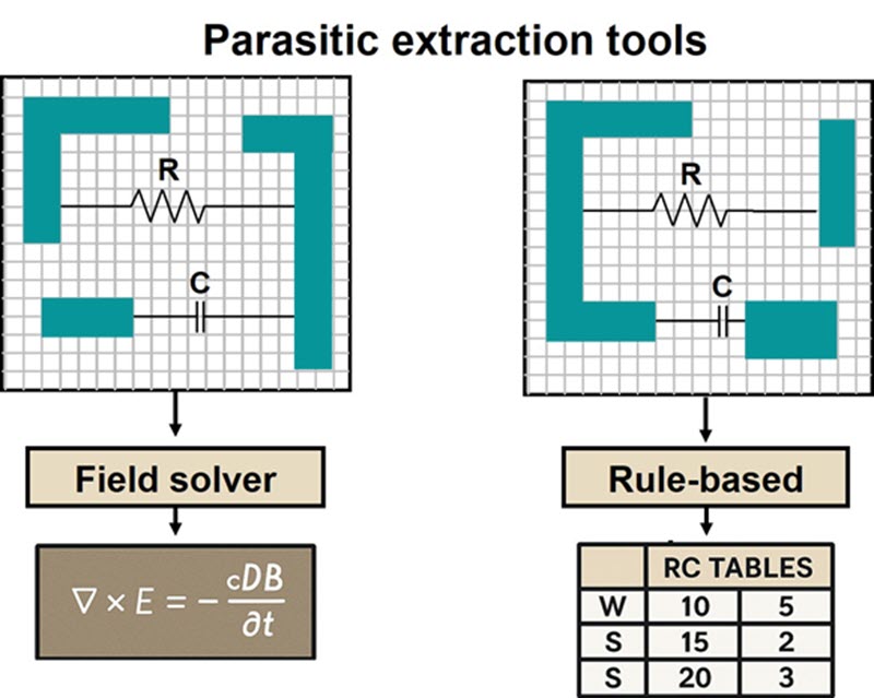
Parasitic extraction tools for semiconductor design are generally divided into three main categories: field solver-based, rule-based extraction and pattern matching, each with its own strengths and suited for different design requirements (figure 2).

Field solvers. Field solver-based approaches use numerical techniques to solve electromagnetic field equations, such as Maxwell’s equations, which allow them to model complex geometries and interconnects with a high degree of accuracy. These methods excel in capturing distributed parasitic, making them particularly useful for designs where detailed insights into electromagnetic phenomena are crucial. This precision is essential for high-frequency circuits, radio frequency (RF) designs, and other advanced applications that demand a deep understanding of parasitic effects to ensure performance integrity. However, the trade-off with field solver methods is their computational intensity. Since they solve complex mathematical equations across fine geometric details, they require significant computational resources and time, especially when applied to large-scale designs. This limits their widespread use in routine workflows, relegating them mostly to specialized tasks where the highest level of accuracy is a necessity.
Rule-based. Rule-based extraction tools, in contrast, operate on predefined models and design guidelines, which allow them to estimate parasitic elements in a quicker and more scalable manner. These tools rely on established rules derived from previous simulations and physical laws, applying them across the design layout to extract parasitic. Although rule-based methods may not capture the same level of fine detail as field solvers, they are highly efficient, offering much faster extraction times and the ability to handle larger, more complex designs without overwhelming computational resources. This makes them the preferred option for most digital and analog IC design workflows, where designers prioritize a balance between speed, accuracy, and scalability. Rule-based tools are particularly well-suited for mainstream applications, where the trade-offs in precision are acceptable, and the design geometries are not as complex or demanding as in high-frequency or RF circuits. These tools are also more user-friendly, requiring less setup and computational overhead, making them accessible for a broader range of design projects.
Pattern matching, often considered a 2.5D extraction technique, helps by recognizing recurring layout patterns in the design. It uses pre-characterized parasitic values for specific geometric configurations to speed up the extraction process without performing complex calculations for each instance. Pattern matching provides a balance between speed and accuracy, making it suitable for large-scale designs that involve repetitive structures, such as standard cells or repeated circuit blocks.
Choosing an extraction tool
The decision between different parasitic extraction tools depends on the specific needs of the design. Field solver methods are ideal for specialized applications where accuracy cannot be compromised, such as in RF, microwave, and millimeter-wave designs, or in advanced nodes with dense and complex interconnect structures. Rule-based tools are the backbone of mainstream design flows, offering a practical and scalable solution for most digital and analog ICs. Pattern matching provides a flexible middle-ground solution, enhancing extraction efficiency for repetitive structures.
Designers must evaluate the performance, resource constraints and the complexity of their designs to choose the appropriate methodology. In many cases, a combination of different approaches may be used: field solvers for critical areas requiring high precision and rule-based methods for the bulk of the design, providing an optimal balance of efficiency and accuracy throughout the design process, and pattern matching to optimize efficiency in recurring design patterns.
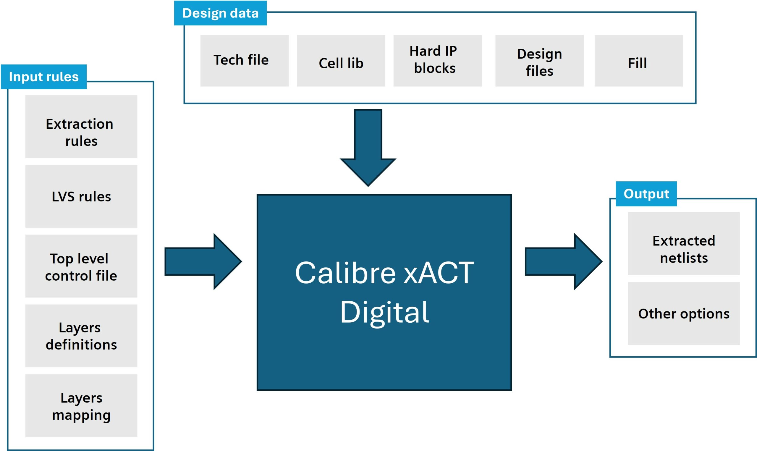
There are tools, including Calibre xACT, that employ both rule-based and field solver approaches, plus offer pattern matching. For most designers, having a tool with high precision in extracting interconnect parasitics such as resistances and capacitances, are critical for understanding IC performance. An advanced extraction tool can capture detailed interactions between interconnects and devices within the IC, offering important insights for optimizing design performance and addressing signal integrity challenges (figure 3).

Conclusion
Efficient parasitic extraction is vital for optimizing IC performance by accurately modeling resistances, capacitances and other parasitic elements. Designers have options when it comes to extraction tools, so should consider one that supports for both analog and digital design flows, can find and mitigate parasitic effects that impact signal integrity, timing closure and power efficiency and is qualified for all design nodes. Precise extraction results help designers make informed decisions early in the design process, ensuring robust and reliable IC development.
Mark Tawfik
Mark Tawfik is a product engineer in the Calibre Design Solutions division of Siemens Digital Industries Software, supporting the Calibre PERC and PEX reliability platform. His current work focuses on circuit reliability verification, parasitic extraction and packaged checks implementation. He holds a master’s degree from Grenoble Alpes University in Micro-electronics integration in Real-time Embedded Systems Engineering.
Also Read:
Revolutionizing Simulation Turnaround: How Siemens’ SmartCompile Transforms SoC Verification
Siemens EDA Unveils Groundbreaking Tools to Simplify 3D IC Design and Analysis
Jitter: The Overlooked PDN Quality Metric
Share this post via:


Comments
There are no comments yet.
You must register or log in to view/post comments.