Executives from the major EDA companies attend the Design Automation Conference to introduce new product features, describe new initiatives and collaborations, meet with customers, and participate in lively conference panel discussions. Daniel Nenni and I were fortunate to be able to meet with Joe Sawicki, Executive Vice President of the IC EDA segment at Mentor, a Siemens business, for a brief update. Here are some of the highlights of our discussion.
Machine Learning in EDA
There were numerous technical sessions and EDA vendor floor exhibits relating to opportunities to incorporate machine learning algorithms into design automation flows. Joe shared some examples where ML is being integrated into Mentor products:
- Calibre Litho Friendly Design (LFD)
Lithographic process checking involves evaluating a layout database for potential “hotspots” that may detract from manufacturing yield. Although conventional design rule checking will identify layout “errors”, there remains a small, but finite, probability that a physical design may contain yield-sensitive topologies at the edges of the litho process window. Traditionally, lithographic process checking utilized a detailed litho simulation algorithm applied to the layout database – a “model-based” approach.
However, that method has become computationally intractable at current process nodes. Instead, a “fuzzy” pattern matching technique was pursued, using a set of “hotspot-sensitive” layout patterns provided in the foundry PDK. A set of “rule-based” checks were applied using these patterns. More recently, a mix of model-based and rule-based techniques are used, where a subset of patterns find layout structures to direct to the litho simulation tool. Yet, pattern identification is difficult. It relies upon the (growing) database of hotspot identification, and a judicious selection of the pattern radius – too large a pattern will result in fewer matches and poor coverage, too small a pattern will identify many unnecessary hotspots for simulation.
Joe indicated, “Machine learning technology has been integrated into the Calibre LFD tool, to better distinguish which pattern structures are potential litho risks using training set learning.”
The figure below depicts a deep neural network applied to the binary classification of design patterns to direct to litho simulation (from the Mentor whitepaper: Elmanhawy and Kwan, “Improve Lithographic Hotspot Detection with Machine Learning”).
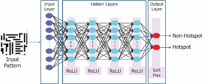
Pattern matching and litho simulation rely upon an existing database of known hotspots. Using a deep neural network, using hotspot and non-hotspot training data, the ML-based approach in Calibre LFD predicts additional yield detractors in new layout, beyond the pattern set in the PDK. Very cool.
- Calibre mlOPC
Joe continued, “We are also incorporating ML technology into the Calibre products used directly by the fabs. There is a wealth of metrology data taken during fabrication. We are applying pattern decomposition and classification on this data to provide feedback to the process engineering team, for process line tuning/centering and for optical mask correction algorithms.”
- Tessent Diagnosis
Lastly, Joe described how ML methods are being applied in the area of fault diagnosis. He indicated, “Mentor has led in the introduction of cell-aware test, where additional circuit node and parametric fault candidates within cells are presented to the test pattern generation and fault simulation tools. We have incorporated ML inference techniques within Tessent Diagnosis to correlate test fail data, and provide improved cell-internal diagnostics to the physical failure analysis (PFA) engineering team.”
There’s no doubt that ML technology will offer EDA developers new techniques for inference classification in analysis flows (and potentially, new approaches to non-linear optimization algorithms in design implementation flows).
Automotive System Verification and Digital Twin Modeling
There continues to be synergistic product developments within Siemens, leveraging the IC design and verification technology from Mentor. (I presume any questions about the motivation behind the Mentor acquisition by Siemens have long since been answered.)
Joe described a recent Siemens announcement – the “PAVE 360” initiative – which provides a comprehensive (pre-silicon) verification platform for simulation of an automotive environment.
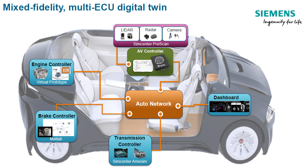
Joe said, “With the Veloce Strato emulation system, we have the capability and capacity to provide a digital twin of the automotive silicon design, the embedded software, the sensor/actuator systems, and the surrounding traffic environment into which the ADAS or autonomous vehicle is placed. This includes both the deterministic and predictive (ML-based) decision support within the model.”
Joe also reminded us, “A digital twin environment is used not only for pre-silicon verification – it is also the debug platform to analyze field data. Testing of autonomous driving solutions will uncover issues, providing engineers with an accident database.”
The ISO26262 standard for autonomous vehicles mandates a closed-loop tracking system that demonstrates how these issues have been addressed and subsequent verified. The PAVE 360 digital twin platform is the means to provide that qualification.
The overall goal of the Siemens PAVE 360 platform is to provide a verification reference solution across the breadth of automotive sub-system suppliers. A number of demonstration labs have been established worldwide, providing suppliers with access to the platform – see below.
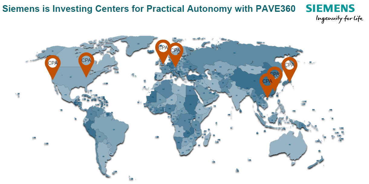
More info on the PAVE 360 initiative is available here.
Photonics
In our remaining minutes, Joe highlighted another recent Mentor announcement, focused on accelerating the design and verification of silicon photonics layouts. Conventionally, layout design consisted of placement of cells from a photonics library, followed by manual custom layout generation of the “waveguides” between the cells (and the related electrical signals that modulate the waveguides). There are strict constraints on the length and curvature of the guides to minimize dispersion – photonic layout design has required specialized layout expertise.
Joe described the new LightSuite Photonic Compiler platform, developed with collaborative support from Hewlett-Packard Enterprise. The compiler provides automated generation of the waveguide layouts and connections, as well as the surrounding electronic component interconnects. The figures below illustrate the overall compiler flow, as well as an example where the electrical connectivity is critical to the proper waveguide function.
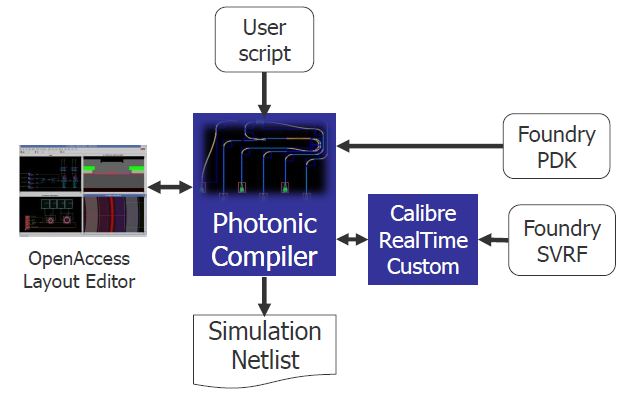
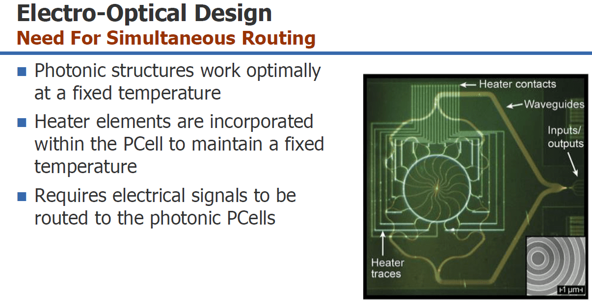
The curvilinear nature of photonic structures necessitates exacting design rule descriptions. Calibre has been extended to support “equation-based” design rules in the foundry’s photonics PDK. Calibre RealTime Custom is exercised within the LightSuite Compiler to ensure the waveguide (and electronic) interconnects are DRC-clean.
Joe indicated, “To date, photonics design has required specialized expertise, utilizing a full-custom methodology. The automation now available offers capabilities that will enable faster implementation. Designers will now be able to do what-if optimizations that were previously extremely difficult.” Mentor quoted a design example with 400 optical and electric components placed, routed, and DRC-verified in 9 minutes with the LightSuite Photonic Compiler. More info on LightSuite is available here.
Although brief, the discussion that Daniel Nenni and I had with Joe S. was enlightening. Machine learning-based classification and optimization approaches to EDA algorithms are well underway, with many more applications to come. Digital twin verification platforms will enable (multiple vendor) subsystems to interact in a replica of a complex external environment, both in pre-silicon validation and post-silicon debug. The opportunities for local, high-speed signal interfacing using integrated silicon photonics are great, but their progress has been hampered by the need to employ a full-custom methodology – improved automation flows will no doubt accelerate this market segment. Occasionally, I find myself thinking, “Oh, there probably won’t be much new at DAC this year.” – then, when at the conference, I never cease to be amazed at the ongoing innovations in the EDA industry.
-chipguy
Share this post via:


Comments
There are no comments yet.
You must register or log in to view/post comments.