Chiplets continue gaining momentum, fueled in large part by applications for AI and 5G/6G RFICs. Keysight has a strong presence at this year’s Chiplet Summit in Santa Clara, which includes Simon Rance in a super panel discussing “Chiplets: The Key to Solving the AI Energy Gap” and Nilesh Kamdar with a keynote on “Using Design-to-Test Workflows and Managing the IP Lifecycle in Chiplet Designs”, as well as several technical talks. Keysight previewed some of its material for the conference, focusing on three aspects of its chiplet integration solutions: system-level electrical layer analysis, a compliance testing strategy to characterize golden die and die-to-die channels, and engineering lifecycle management for chiplet design.
System-level analysis of signal integrity crucial for chiplets
Chiplet designers are facing many challenges in creating die-to-die interconnects. Do teams align with a specification, such as Universal Chiplet Interconnect Express (UCIe), Bunch of Wires (BoW), or others? Do they follow the details of a chosen specification closely, seeking to capture the economic benefits of interoperability, or do they customize some features, tuning interconnects to optimize performance and power consumption? In any chiplet design scenario, system-level chiplet signal integrity analysis determines a design’s outcome. Packaging for 3D heterogeneous interconnect (3DHI), using standard or advanced packages specified in UCIe, becomes more than a mechanical convenience, affecting high-bandwidth signals.

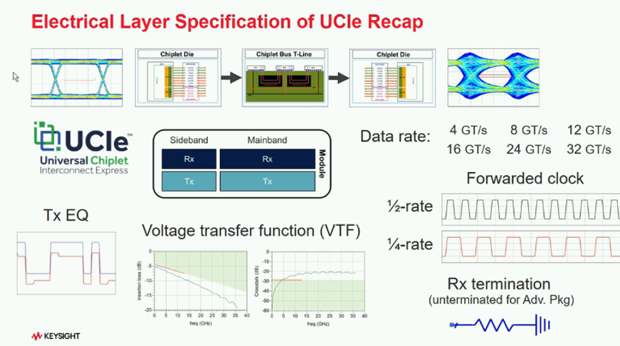
Preventing suboptimization of one signal metric while potentially degrading others calls for detailed, system-level electrical layer analysis, evaluating all metrics simultaneously. Keysight’s Chiplet PHY Designer, an extension to Keysight Advanced Design System (ADS), provides robust system-level signal integrity analysis for chiplet interconnects, including UCIe and BoW. It updates its analysis incrementally as schematic and layout details change.
Tim Wang Lee, Ph.D., Signal Integrity Application Scientist at Keysight, presents the topic “Fast Track Chiplet Integration with Streamlined UCIe Electrical Layer Analysis” in the Integration sessions. “UCIe specifies the voltage transfer function (VTF), forward clocking, eye mask equalization, loss, and crosstalk level,” he says. “Our software does the work by setting up TX and RX termination equalization and analyzing and visualizing VTF crosstalk and loss masks for different data rates.”

Dr. Tim also says the visualization tools in Chiplet PHY Designer help spot the root cause of issues, such as insufficient trace spacing creating coupling and excessive crosstalk or channel lengths contributing to losses. He emphasizes that while Chiplet PHY Designer is UCIe-aware, it also handles analysis for BoW or customized die-to-die interconnect links.
Die-to-die interconnect test and characterization
UCIe leans heavily upon work done for its board-level predecessor, PCIe, with modifications recognizing its die-to-die context. However, there is one significant difference – compliance testing. PCIe is famous for its plugfests, where teams can take chips designed with mature PCIe IP blocks, mount them on circuit boards, install them in systems, and stage physical and protocol measurements using signal generators, oscilloscopes, and bit error rate testers. UCIe presents a different challenge since fabricating a chiplet prototype is much more expensive than making a board prototype, and limited test point visibility can make probing infeasible.
Pedro Merlo, Manager of Strategic Planning at Keysight, comes from the test instrumentation side of the house and has been focusing on die-to-die interconnects for the past two years. “Keysight is a proud contributor to UCIe and BoW, the two most prominent chiplet interconnect standards,” says Merlo. “The vision is to base compliance testing at the physical and protocol layers on a ‘golden’ die.” But does such a die exist, especially for customized link designs? For an open chiplet ecosystem to develop, at least three components – one die, one interconnect structure, and another die that completes the link – must be testable standalone and swappable for another test article.
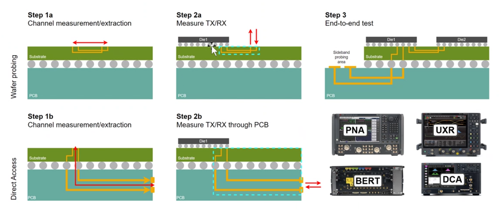
Merlo’s tutorial in the Pre-Con D: Introduction to Die-to-Die Interfaces session shares some in-progress thinking where Keysight’s unified measurement science – equivalent methods between test hardware and EDA software – comes into play. “We can use our high-precision benchtop test equipment to characterize a chiplet’s built-in self-test (BIST) and measure transmitter amplitude, slew rate, jitter, skew, equalization, sensitivity, and more,” he begins. “Our objective is to test as much as possible to reduce the uncertainty, especially after packaging, when test points are no longer accessible.”
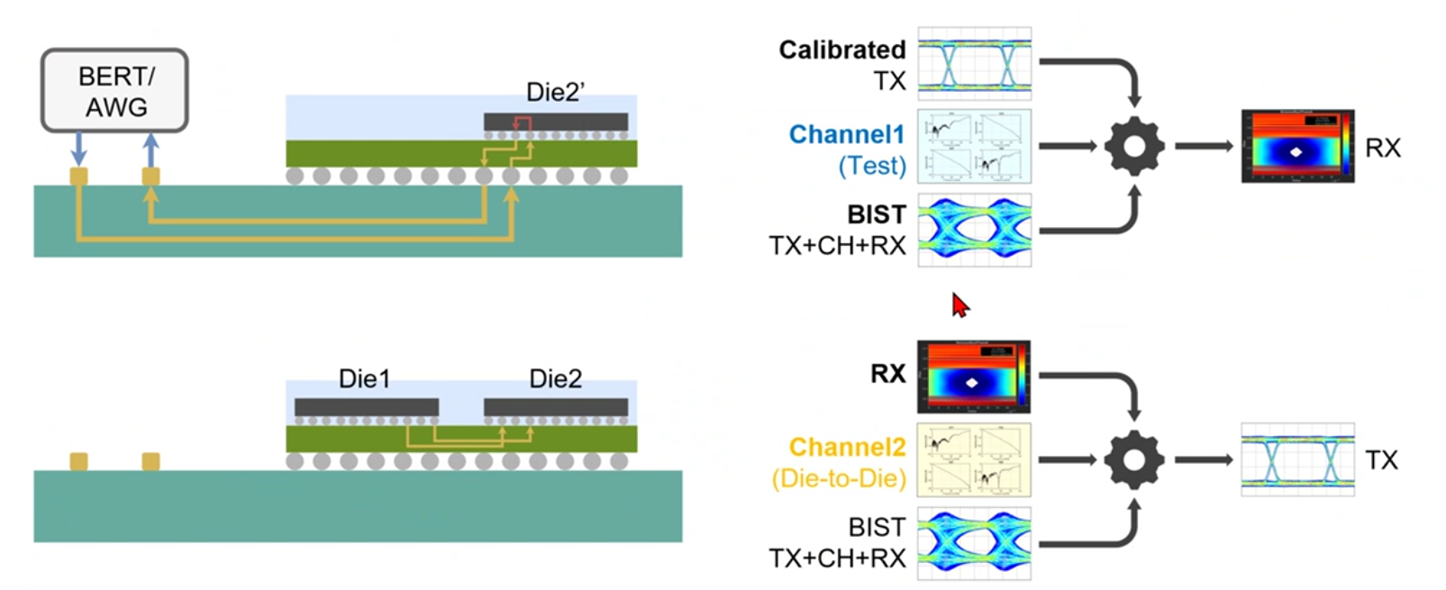
“We’re proposing extracting channel characteristics and factoring them into measurements made at the far end of the transmitter, then using those characteristics in a model for end-to-end tests,” Merlo continues. “The approach adds test points to a substrate, makes measurements there, then subtracts out channel effects to see what the signal looks like at the receiver microbump.”

Merlo points out that BIST results can tell designers that a link works but not how much margin it has or where a problem might be. Decomposing the BIST into two phases provides a method for examining links closely.

More importantly, decomposing the BIST paves the way for simulations with robust models to produce results equivalent to measurements. “By breaking the link into pieces and ensuring each one works and meets specifications, we get better information,” Merlo concludes.
Engineering lifecycle management for chiplet design
Considering both electrical and mechanical nuances, chiplet design presents a more significant enterprise opportunity for engineering lifecycle management (ELM) than SoC design. While today’s focus on chiplet design is internal, teams may soon be considering if third-party chiplets are candidates for integration. There’s also reuse of chiplets to consider, and if an organization has more than one design team, there needs to be an easy way to store and share design information across teams.
“Think of chiplets as systems,” says Pedro Pires, ELM Solutions Engineer at Keysight. “Chiplet design carries system engineering connotations – there are die, interposers, packages, and artifacts around each component, some internally sourced and some procured from third parties.” Pires says a common chiplet design scenario will see teams starting with specifications, diving into a catalog with parameterized search and compare of components, and creating a bill of material (BOM) with built-in traceability of assets.

Metadata around chiplets in Keysight Design Data Management (formerly known as Cliosoft SOS) can include what versions exist, where they are in use, and their technical characteristics, including electrical, mechanical, and application programming interface (API) information, making it easy to highlight differences. “HUB can provide critical alerts such as release conflicts, where one bill of material contains different versions of a chiplet somewhere in its hierarchy, or notify designers of a newer version,” adds Pires.
There may be more steps for designers than just grabbing an asset from the catalog. Pires points out that selecting third-party chiplets may require team members to execute non-disclosure and licensing agreements. Keysight ELM implements workflows as a mechanism to automate approval and enforcement policies, with built-in activity reporting for internal and third-party audits. Beyond these customizable workflows, granular access controls can gate access to resources based on user characteristics, roles, or locations, which is essential for expert control scenarios.

Keysight ELM introduces a data-agnostic methodology for managing the entire lifecycle of chiplets and offers creative ways for various roles beyond design teams to share and manage information. It integrates seamlessly with many chiplet design tools, including Keysight ADS and Cadence Virtuoso, via a REST API. It also connects with familiar tools like Jama, JIRA, Bugzilla, Confluence, and more.
Learn more at Chiplet Summit 2025
The complete technical presentations will reveal more details for Chiplet Summit 2025 conference attendees. In addition to the speaking slots on the program, exhibitor attendees can see Keysight’s chiplet integration solutions in booth #307, including the presentation on ELM. For more information on Chiplet PHY Designer, Keysight Design Data and IP Management, and the Chiplet Summit program and registration, please visit the following:
Keysight W3650B Chiplet PHY Designer
Keysight Design Data and IP Management
Also Read:
GaN HEMT modeling with ANN parameters targets extensibility
Keysight EDA 2025 launches AI-enhanced design workflows
Webinar: When Failure in Silicon Is Not an Option
Share this post via:


Comments
There are no comments yet.
You must register or log in to view/post comments.