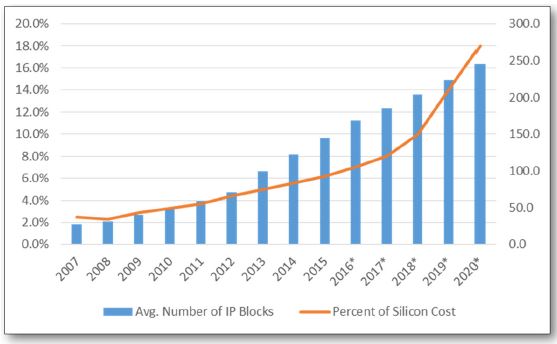
 The recent growing complexity in SoC designs attributed to the increased use of embedded IP’s for more design functionalities, has imposed a pressing challenge to the post-silicon bring-up process and impacting the overall product time-to-market.
According to data from Semico Research, more than 60% of design starts contain IP reuse and the number is expected to increase due to the high silicon demand related to today emerging applications such as 5G wireless communication, autonomous driving and AI.
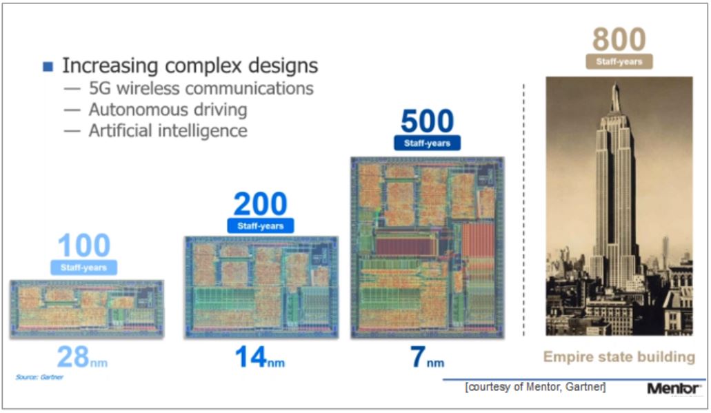 Based on data from Gartner, the staff-years equivalent effort for designing a 7nm SoC is more than 5 times than those of 28nm. The cost to testing the associated IPs is also on the rise. To mitigate this post silicon validation and debug challenge, design teams have resorted in applying on-chip debug strategy, more automated techniques for post-silicon test generation and pre-tapeout assertions for effective coverage/analysis. For example, on-chip buffers is deployed to improve observability and controllability of the internal signals during trace-based debugging.
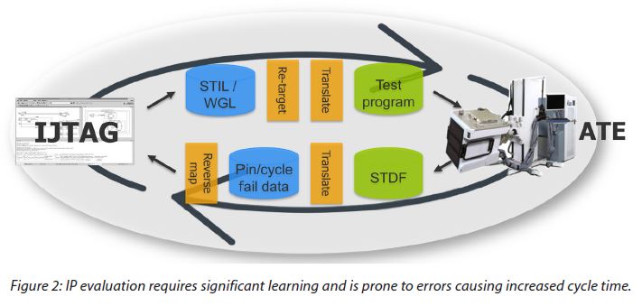 The traditional silicon bring-up and debug flow has been inherently inefficient as it involves multiple translations of test related collaterals. In this scenario, a DFT engineer or designer initially uses a mix of document based test descriptions and simulation generated tests to handoff the testing directives to the test engineer, who will then reformat them to the ATE of choice for silicon validation. The subsequent test generated results is then re-translated back into tool format used by the DFT engineer for review. Such iterative process is prone to delays as access to testers may be interrupted while run data being process for assessment.
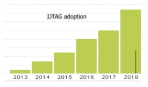
IJTAG (Internal Joint Test Action Group) or IEEE 1687 provides an access standard to the embedded instruments and allows vector and procedural retargeting. It incorporates the mainstream IEEE 1149.1-x and the design-for-test standard IEEE 1500. Since its introduction in 2013, the IJTAG based adoption has been on the increase. The JTAG TAP (Test Access Port), a five-pin, state-machine based interface, not only controls the boundary-scan logic and tests, but it has been used to access more embedded instruments and IPs. 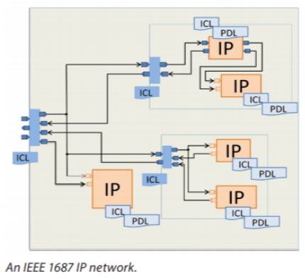
IJTAG creates a plug-and-play integrated environment and use of the instrumentation portions of IP blocks which includes test, debug, and monitoring functions. Part of the standard includes two languages: first, ICL (Instrument Connectivity Language) hardware rules related to the instrumentation interfaces and connectivity between these interfaces; and second, a Tcl-based PDL (Procedural Description Language) that defines operations to be applied to the individual IP blocks. While ICL is an abstraction of the design description needed to scan read/write from/to the instrument, PDL defines the syntax and semantics of these operations. The PDL may be written with respect to the instrument’s I/Os and is also retargetable. Retargeting translates the operations from the instrument through hierarchical logic described in ICL up to the top level of the design.
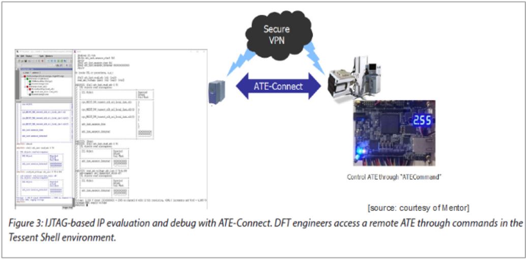 Even though IJTAG streamlines IP integration during the design phase, frequent third party related IP evaluation and debug issues still persisted during silicon bring-up –thus affecting the production yield ramp-up. To address this issue, Mentor’s Tessent SiliconInsight with ATE-Connect™ technology paired with Teradyne’s PortBridge for UltraFLEX, to enable DFT engineers to directly control and observe IPs in the SoC-under-test on the ATE. This solution resolves a number of key problems of an IJTAG-based IP evaluation and debug. It delivers a protocol-based flow instead of a pattern-based flow using IJTAG commands, and utilize Tcl-based Tessent shell interface to access ATE unit remotely through TCP connection. Another Tessent’s tool SimDUT to allow users to debug and validate the PDL procedures and related Tcl procedures
Figure 4 shows an example on how the environment is being utilized. The MBIST engines at the upper right are being accessed and controlled through the IJTAG. Similarly, the debug of two mixed signals IP blocks, DAC and ADC can also be achieved through the same approach. Tessent SiliconInsight tools could address both the test engineer need of having a fast and reliable test to optimize yield and minimize test cost, and the DFT engineer interest in confirming the functionality and critical metric extraction.
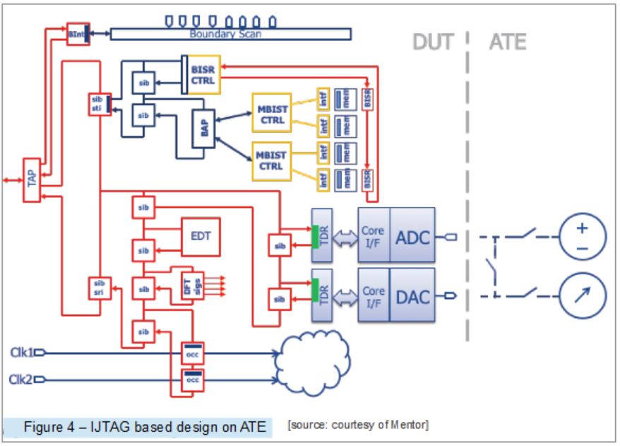 Initially, the test engineer can configure the ATE and perform proper setup/biasing of the DAC/ADC blocks. Once setup is completed, the test engineer passes control to the DFT engineer to run the previously designed tests or to do any needed interactive debug. Upon verifying both IP blocks, the external ATE resources can be optionally replaced with a less costly loopback connection mode. Running subsequent what-if testing, applying different adjustment on the adjoining block such as PLL and reassess system level functionalities can be done. Both the DFT and test engineers viewpoints are aligned (while they might not in the same geographical locations), enabling also pattern generation need or using ATE-Connect to target a bench setup with the debugged tests –streamlining further the three environments (design, test, bench) to accelerate time-to-market.
The takeaway from having Tessent SiliconInsight with ATE-Connect technology is that it delivers efficiencies in silicon bring-up, post-silicon and IP debug or evaluation. The simplified IJTAG based standard also provides DFT and test engineers with option to scale their IP testings.
For more info on Tessent based test flow, check HERE.
Share this post via:


Comments
There are no comments yet.
You must register or log in to view/post comments.