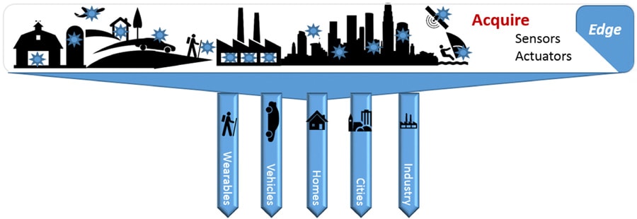
The IoT market opportunities in segments like wearables, vehicles, home, cities and industrial are all growing thanks to the combination of semiconductors, sensors, software and systems technology. New hardware designs for IoT edge devices appear on a daily basis, and the companies behind these new products can often be start-ups or just a handful of people in a larger company doing something totally different. Of course to run a successful business you have to manage cash flow, so ideally when starting a new IoT project the expenses need to be managed closely during the design phase. Maybe you need to get an early IoT prototype completed as proof of concept in order to secure funding for production.
IC Insightsproduced a report in June 2017 that showed that the IoT market size in 2016 was $74.6 billion, project to reach $124.1 billion by 2020 in the five categories mentioned above. The IoT edge market doesn’t include gateways, servers, computers, smartphones or tablets.
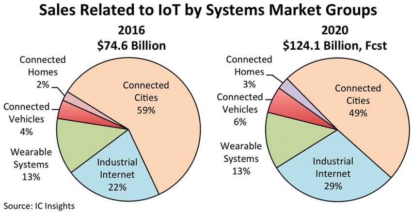
The five IoT market segments fuel semiconductor revenue in the following proportions where smart cities is the largest segment at 59% or $10.82 billion, followed by Industrial IoT at $4.02 billion and connected vehicles at $2.14 billion:
![]()
Custom SoCs are a popular IoT implementation approach for edge devices in order to get the most battery life, performance, lightest weight or smallest sized product. Alternate approaches like placing discrete components on a PCB may not meet requirements. Using a custom SoC does provide several benefits over discrete parts, like:
- Lower BOM costs
- Smallest size
- Lowest power, longer battery life
- Higher performance
- Better reliability
- No more obsolete components
- Greater IP protection, harder for competitors to copy
- Higher barriers to entry for your competitors
Before you get all enamored with the idea of developing a custom SoC it is wise to consider your costs, market size and segmentation, time to market, your competitors and the proper process node. Fabricating with a 180nm node is much cheaper than choosing to use 28nm, plus with 180nm you still use 3.3V supplies which provide a high dynamic range and better noise margins, something quite useful for RF antennas.
You’ll hear terms like Non-recurring Engineering (NRE) which include the price of EDA design software, semiconductor IP blocks from 3rd parties and the first silicon run to get your samples. Mentor – a Siemens business, provides a 30 day, no cost evaluation of their Tanner EDA tools for design and simulation of your custom SoC.
- Schematic capture of AMS design using S-Edit
- Processor IP – Arm Cortex-M0 or Arm Cortex-M3
- Analog simulation using T-Spice
- Digital simulation using ModelSim
Once your proof of concept is ready the next step is to begin implementation using software tools and semiconductor IP. Here’s the flow from Mentor:
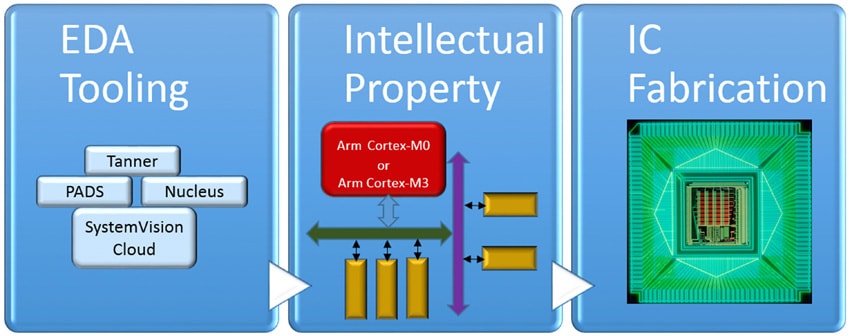
Pushing down into the EDA tooling box there are four distinct engineering tasks:
- IC design
- Embedded Software
- System Exploration
- PCB Design

Analog Mixed-Signal (AMS) design and MEMs design are done with the Tanner EDA tools, and this is also where you model all of the IoT sensors. Here’s more detail on what the AMS IC design flow looks like:
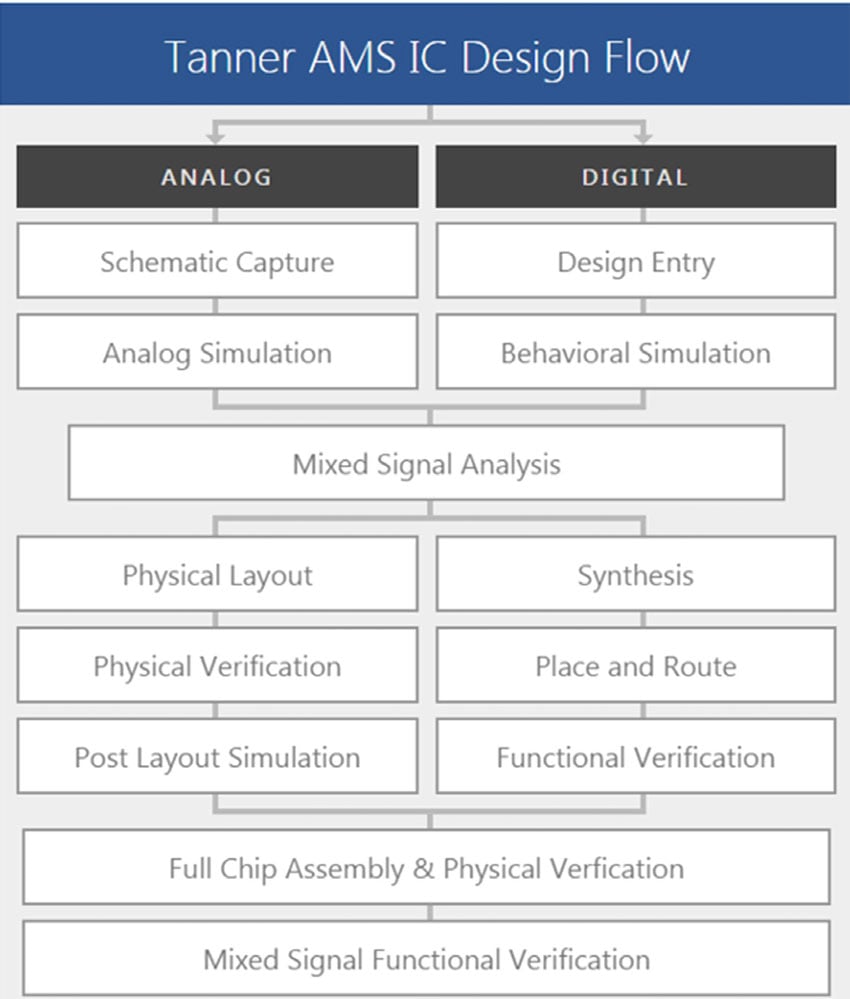
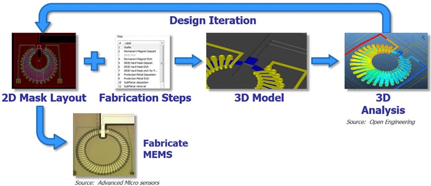
If you’re IoT device needs to measure something like pressure, rotation, acceleration, speed or humidity then MEMS can be modeled in 2D and 3D then analyzed for physical effects.
For embedded software development Mentor Embedded has a real-time operating system (RTOS) and other tools for IoT edge devices. The Nucleus RTOS is well-equipped for battery powered IoT devices and has been used in some 3 billion devices so far. During embedded software development you would use Sourcery CodeBench:
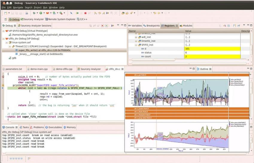
With Sourcery CodeBench your team can use micro-controllers or microprocessors, then understand system execution, measure performance and even debug your apps.
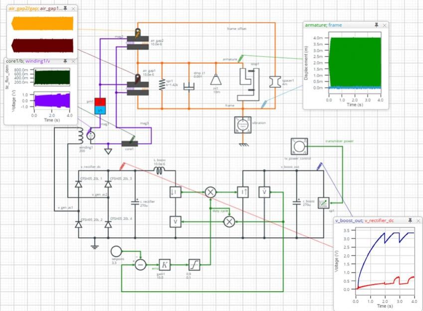
For system-level design and documentation Mentor has the SystemVision Cloud tool that can model both electronics and mechatronics systems, then simulate them so that you can explore the best design approach.
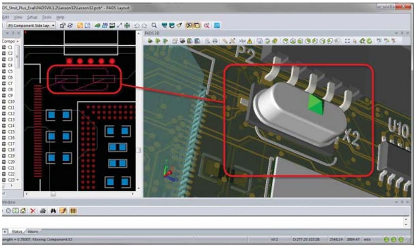
To finally place your SoC and sensors onto a PCB it’s time to use software called PADS Standard, which has both schematic capture and board layout features at an affordable price.
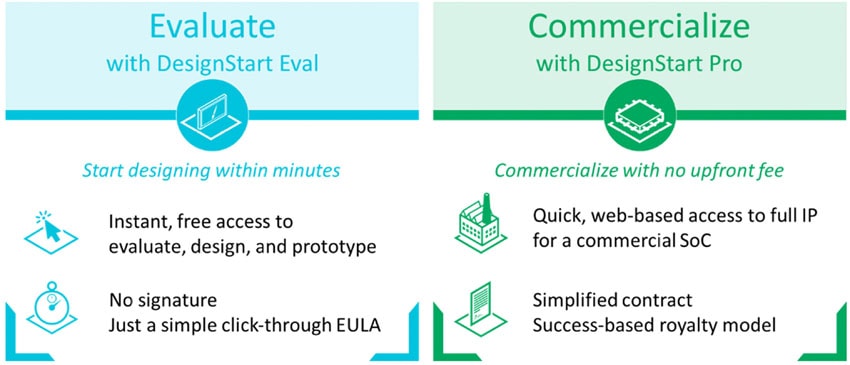
The most popular processor architecture in the world comes from Arm and they have put together a program called DesignStart Evalthat allows you to design and prototype at no cost, then when you’re ready for production you upgrade to DesignStart Pro.
Having IC samples produced at a low cost can be accomplished with multi-project wafers (MPW), where you are sharing the IC mask costs with other companies onto the same silicon wafer. Foundries and companies like MOSIS, eSilicon and EUROPRACTICE can assist you with the MPW logistics. It costs about $16K to get 45 IC samples on a 180nm process, according to EUROPRACTICE, while the second order of 45 samples has an even lower price of $2K.
Your particular SoC for IoT applications may have unique requirements that drive up the cost like adding more IP blocks, including design consulting, needing a smaller geometry process, needing more EDA tools, PCB fabrication, or more analysis of MEMS.
Full production is the final step after your proof of concept has been accepted and raised enough capitol, so you choose a foundry partner and get quotes for mask costs and production. At the 180nm node you can expect mask costs to be around $150K, while more advanced nodes like 90nm you can expect mask costs of $500K.
Summary
The IoT market is very promising and with the right approach you can minimize engineering costs for both a proof of concept and into production using vendors like Mentor and Arm.
There’s a 14 page White Paper from Mentor on this topic, available to download.
Related Articles
- IoT Project Planning – Profiting from the Folly of Others
- Arm and Mentor Use DesignStart Program to Accelerate Proof-of-concept for IoT Designs
- Fusing CMOS IC and MEMS Designs for IoT Edge Devices


Comments
3 Replies to “Developing Affordable IoT Systems”
You must register or log in to view/post comments.