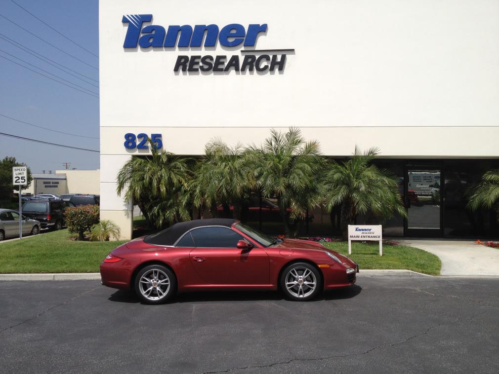
 Rarely does a month go by without acquisitions in the fabless semiconductor ecosystem. Not surprisingly one of the most read pages on SemiWiki is the EDA Merger and Acquisitions Wiki with more than fifty seven thousand views. It really is a nice family tree, one which we (Daniel Payne) are diligent on keeping current. One of the most accretive EDA acquisitions this year in my opinion is Tanner EDA and I will tell you why.
EDA Mergers and Acquisitions Wiki – SemiWiki.com
IoT Lacks Tools, Says EDA Vet
The above is a recent headline of an EETimes article featuring Alberto Sangiovanni-Vincentelli, a Berkeley professor and co-founder of EDA giants Cadence and Synopsys.
“The Internet of Things is just an intermediate step on the way to the sensor dominated world” where the numbers of networked sensors will exceed the population by several orders of magnitude, said Alberto Sangiovanni-Vincentelli, a Berkeley professor and co-founder of EDA giants Cadence and Synopsys.
“My passion is the science of design. I hate seat-of-the-pants design, leaving engineer free to design is a recipe for disaster,” he said. “What excites me is abstracting the meaning of a design and applying it to everything,” he added.
This may certainly apply to Berkeley, Cadence, and Synopsys but it does not apply to Caltech and Tanner EDA. There is a “Brief History of Tanner EDA” which traces their roots back to Caltech and Carver Mead’s seminal textbook on VLSI design HERE. While I understand Alberto’s points, I’m more of a seat-of-the-pants guy and believe the majority of the IoT designs will be from small to medium sized groups of entrepreneurs which will also consist of seat-of-the-pants kind of people.
An example of an IoT design is MEMS (Micro-electro-mechanical systems) where very small devices such as sensors, gyroscopes, accelerometers, and resonators are integrated into an SoC for IoT applications. Tanner EDA is all about MEMS and has a nice video, webinar, and whitepapers to get you started:
Micro-electro-mechanical systems (MEMS), is the technology of very small devices, such as sensors, gyroscopes, accelerometers and resonators. Whether your design is purely MEMS or a combination of MEMS and IC SoC, these tools can meet your most challenging needs. Thisvideo introduces the Tanner tool flow for MEMS design.
Tanner MEMS Tool Suite Overview and Demo; Thiswebinarwill show how Tanner L-Edit MEMS Design and SoftMEMS™ 3D Solid Modeler can be used to shorten your design cycle and improve the manufacturability of your MEMS devices.
Meeting MEMS Design Challenges with Unique Layout Editing and Verification Features–Part 1: A big difference between MEMS layout and IC layout is the use of unique, irregular shapes. Unlike conventional CMOS IC design, where layout shapes are usually Manhattan style (such as rectangles and rectilinear polygon) or polygon with 45-degree edges for routing, MEMS design utilizes a much broader variety of geometries, due to its wide application in mechanical, optical, magnetic, fluidic and biological fields. This two-part paper describes how and why support and ease of use for implementation of irregular shapes, including curves and all-angle polygons, is a critical criterion differentiating MEMS-oriented CAD tools from conventional IC-oriented tools. (Part 1focuses on layout editing;Part 2on verification.)
The bottom line is that Tanner EDA made AMS tools both affordable and easy to use, two things that are critical in the developing IoT market. If you ask me that is why Mentor acquired Tanner EDA and is keeping the brand as a separate business unit, absolutely.
Share this post via:


Comments
There are no comments yet.
You must register or log in to view/post comments.