In the name of blogging and increased transparency lets talk about wafer allocation, because it’s coming, believe it. There is already a significant delta between wafer demand and manufacture due to record low inventory levels and the exploding semiconductor demand in China. Both TSMC and UMC posted good July sales numbers: TSMC realized a 17.9% jump from June, UMC a 6.97% jump. In difficult economic times the strong get stronger, as TSMC definitely has, as the 2009 market share data will definitely show.
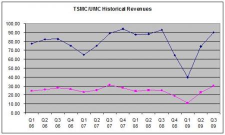
Instead of favoring large customers at the expense of smaller ones, foundries will look at a customers’ forecast accuracy as a basis to judge which could most likely afford less wafers. So an allocation will run across most semiconductor market segments around the world.
This of course spells opportunity for second source foundries (UMC, SMIC, Chartered Semi, Global Foundries), but the key questions are: Where will customers get the already thin engineering talent to migrate design layout to a second source? Will second source foundries offer migration services? Will the customers do it in-house? And unless it is a highly automated process, will the actual migration take longer than the allocation?
Several of the top semiconductor companies already use second, and even third source manufacturing due to the massive volumes required. Most companies use home-made scripts that manipulate layout then use brute force layout design work to cleanup the remaining mess. With new process nodes however (65nm & 45nm), these methods break as the process rules are much more complicated. Commercial tools for the “automated layout modification” required for second sourcing semiconductor designs can yield a 5-10X productivity increase, saving both time and precious engineering resources.


Michael Reinhardt literally wrote the book on this and pioneered the design migration market with his company RubiCAD. Unfortunately RubiCAD’s erratic business practices were not scalable, forcing the company to fold in 2004 after a debatable patent challenge by an unknown company. The dominant player in this market is Sagantec, which I worked for back in the late 1990’s, so I know this business the hard way.

Sagantec, known for giving away nice shirts at trade shows, is a true EDA survivor. Originally a European based research and development operation, Sagantec emerged as a commercial EDA company backed by Isreali venture funds, now with headquarters in Silicon Valley, development in the Netherlands, and sales/support offices in Japan, Taiwan, Korea, and India. Once valued at $50M+, Sagantec got trampled during the DFM gold rush and was forced to clean house in 2008. Now completely remodeled and refocused on the mixed signal / custom IP migration market, Sagantec is profitable, has a healthy backlog, and counts top fabless semiconductor companies and IDMs asactive customers. Case in point from the Sagantec #46DAC demo:
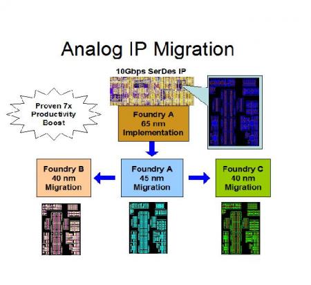
Unfortunately, moving a mixed signal design or custom IP to different foundry process nodes is not, and will never be a trivial matter. This is an extremely difficult job that will require a broad range of experience in design, migration, as well as process technologies. In fact, 80% of the challenge is the technology set-up file, the rest is push-button iteration, improving quality of results. If you think about it, which I have, the mixed software licensing and services model is key here, as well as a gain-sharing business model.
Contact Sagantec for more details and a nice shirt!


Musk’s Orbital Compute Vision: TERAFAB and the End of the Terrestrial Data Center