 If you are a Mentor user, U2U, the Mentor User group is coming up on April 10th. This is an all day event at the DoubleTree. The event is free. Registration starts at 8am and the agenda itself starts at 9am. There is a reception from 5-6pm in the evening.
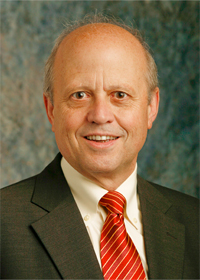
 There are three keynotes. At 9am: Wally Rhines, CEO of Mentor. The Big Squeeze. For decades, we’ve known it was coming and now it’s here. Moore’s Law—which is really just a special case of the “learning curve”—can no longer drive the 30% per year reduction in cost per transistor, beginning with the 20/16/14 nm generation. Either we find innovations beyond just shrinking feature sizes and increasing wafer diameter or we slow our progress down the learning curve, introducing innovative new electronic capabilities at a slower rate than in the past. There are lots of alternatives, including a reduction in profitability of the members of the supply chain, to keep the progress continuing at the same rate as the last fifty years.
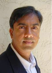
 At 10am: Ashok Krishnamoorthy, the chief technologist at Oracle (the part that used to be Sun Microsystems). Optical Interconnects at a Turning Point – The Opportunity and Prospects for Silicon as a Photonics Enabler. Interconnect will play a major role in overall system performance and energy consumption for future computing systems. Current optical links can provide the required bandwidth, but are relatively expensive and power-hungry. VCSEL-based optical modules can improve the situation greatly, and will help optical interconnects penetrate deeper into computing systems. Recent advances in high-density, ultra-low energy silicon photonic links are likely to make them the preferred solution in the long term as density, bandwidth, and energy efficiency are jointly optimized.
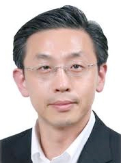
 At 1pm: Shawn Han, VP Foundry Marketing at Samsung. Solutions to Smart Mobile Devices. Samsung have done a great job in becoming a real force in foundry, most famously making most of Apple’s Ax chips. Expect them to be come even more of a force at 16nm. This is billed as a “special session” rather than a keynote so I have no idea what to expect.
Outside the keynotes, the day is organized into 8 parallel tracks: Calibre I and II, CustomIC/AMS, Place & Route, Silicon Test and Yield Analysis, Functional Verifications, PADS, PCB.
Some talks that look especially interesting looking are:
- How to achieve fast power and ground analysis at the full chip level (Broadcom)
- How to design and verify silicon photonics components (University of British Columbia)
- How to take advantage of the TSMC9000 IP reliability program (TSMC Technology)
- Achieving required power, performance, area (PPA) on ARM cores (ARM)
- How Sherlock Holmes and Dr. Watson Track Down a Yield Limiter (Aptina Imaging)
The full detailed agenda is here(pdf). Free registration is here.
More articles by Paul McLellan…


Comments
There are no comments yet.
You must register or log in to view/post comments.