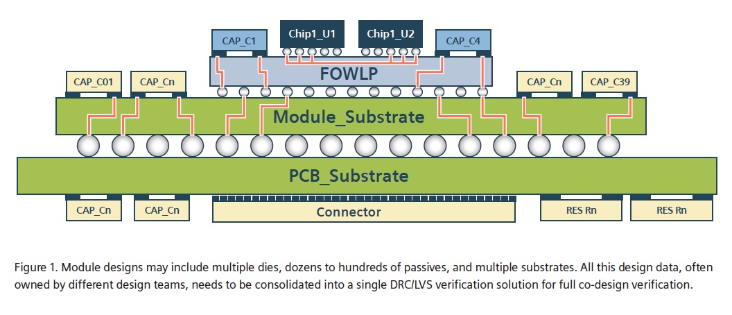
Multi-chip modules are now more important than ever, even though the basic concept has been around for decades. With The effects of Moore’s Law and other factors such as yield, power, and process choices, reasons for dividing what once would have been a single SOC into multiple die and integrating them in a single module have become extraordinarily compelling. These system in package (SIP) modules are becoming ever more popular. Yet for all their advantages, they do add a level of design and verification complexity that must be addressed.

There are many good reasons to use SIP modules. SIP modules let designers break up large die into several smaller dies, which lessens the impact of a fabrication defect. Instead of throwing away an entire large die, only the smaller die affected by a failure need to be replaced. Also, some parts of a large system can easily be fabricated on a lower cost and less technically complex die based on a trailing process node. Similarly, memories, RF and other specialized functional units can reside on their own die using any needed process technology such as NAND memory, GaAs, etc. High speed SerDes for off-chip links can also use legacy analog nodes to save costs and reduce design risk. SIP modules also reduce PCB component counts and simplify board design.
On the flip side, these benefits come with increased complexity. They introduce a new level of interconnect that needs to be verified for correct connectivity. Substrate connections from each die need to be logically correct, and also the geometry of the connections require verification. The pad centers need to be checked for proper alignment. Device scaling and orientation are factors that can determine if the final fabricated parts are functional. Different die and elements used to construct SIP modules have unique thermal properties which can affect the integrity of the bump to pad connections. All of this calls for a solution to ensure that the design is correct.
To help design teams deal with the added complexity of SIP module verification, Siemens EDA has developed a tool called Xpedition Substrate Integrator (xSI) that provides an integrated solution for defining and consolidating all pertinent module design data, allowing for the definition of the golden design intent. There is native integration with Calibre 3DSTACK to provide robust automated DRC/LVS checking for SIP modules. Justin Locke from Siemens has authored a white paper that describes the need for a DRC/LVS specifically targeted at SIP modules. The white paper is titled “System-in-Package/Module Assembly Verification”.
There are several unique challenges that are faced by SIP module verification tools. Because it sits at the nexus between board and die, the task of verifying SIP Modules has to interface with multiple tool flows and also multiple design teams. This data and organization complexity has to be a primary focus for any tool. Additionally, during earlier stages of the flow, the full GDS may not be available to help locate and identify the pads on the die. Siemens xSI offers the ability to create dummy die information that can be used in the interim until the full GDS information if available. Once GDS for the die is available, it can be used to ensure proper pad centering and connection overlap.
System in Package is here now. Design teams need to work with them to deliver market winning products. Today’s SIP modules are a far cry from the old multi-chip modules. It comes as a relief that there are tool solutions tailored to help deliver high quality finished products. The full Siemens white paper is available for reading on the Siemens website.
Also read:
MBIST Power Creates Lurking Danger for SOCs
From Now to 2025 – Changes in Store for Hardware-Assisted Verification
DAC 2021 – Taming Process Variability in Semiconductor IP
Share this post via:


Comments
There are no comments yet.
You must register or log in to view/post comments.