 Of all the things that designers have to worry about in the power-performance-area (PPA) equation, the most challenging is power. SoCs have reached a point that we can put a lot of stuff on them, but if we are not careful we cannot light it all up at once. Dark silicon, where we put subsystems on a chip but then don’t have enough power budget to turn them on, is a real issue.
So as a sort of year-end review, here are lots of the approaches designers take to reduce power:
- low power processes. For planar processes, leakage power has become a real problem and foundries like TSMC and GF have specia low-power variants of their processes with less performance but less power, typically optimized for the mobile market. With FinFET processes, leakage is less of an issue (one of the big reasons for going to FinFET in the first place) and the transistor architecture is less flexible so it looks like they will come in only one flavor
- multiple V[SUB]t[/SUB] libraries. Synthesis tools will automatically use the low power cells except one critical paths that can’t meet timing without using the higher power (and higher leakage) cells
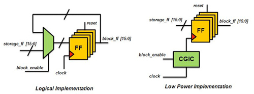
 clock gating. All synthesis tools can replace multiplexors for recirculating data values in a register with a clock gate cell that simply inhibits clocking the register
- automatic sequential power reduction at RTL level. Several EDA companies have tools that will rework the RTL, especially for datapaths, to reduce power by not clocking registers where the results will not be used and so on
- turn the clock off. the simplest way to reduce dynamic power on a functional block when it is not required is simply to stop clocking it. But care needs to be taken with the power delivery network when turning a block back on since the sudden increase in power can cause voltage droop and transients
- power down the block. the challenge here is to make sure that all outputs are tied off properly so that there is not a lot of crowbar current by gates drifting between 0 and 1. And if there is data in the block that needs to be preserved, then special retention registers must be used. Even more so than in the clock case, a lot of care needs to be taken when powering up the block or the inrush current can cause problems all over the chip. Typically the block is powered up with relatively small transistors (so it takes time) and the big transistors are only turned on once the block is already up to normal voltage
- dynamic voltage and frequency scaling (DVFS). vary the frequency of the clock to a subsystem (typically a microprocessor). But this needs to be done with care. First the frequency must be lowered and then the voltage can be. And when getting back up to full speed, first the voltage must be increased and then the frequency can be changed
- race to halt. sometimes running the microprocessor as fast as possible is the way to go. once it is idle again then the rest of the system can be powered down. running the microprocessor slowly may save power in the processor itself but if it means a lot of other blocks have to be powered up for a long time that might be the wrong tradeoff
- make sure that the embedded software turns off whatever can be turned off. It is sometimes the case that the embedded s/w engineers don’t really understand IC power issues, and the IC designers don’t understand embedded s/w and a a lot of power is wasted in the gap. Virtual platforms can play a role here.
- Unique approaches: ARM big.LITTLE, NoCs that can wait for blocks to power up, Cyclos resonant clocks, asynchronous signalling
More articles by Paul McLellan…
Share this post via:


Silicon Insurance: Why eFPGA is Cheaper Than a Respin — and Why It Matters in the Intel 18A Era