Engineers have this fascination with how things work. They are thrilled to tear stuff apart, and sometimes to even be able to put it back together afterwords. So I can keep my recovering engineer card, I thought I’d take a few moments and look inside a technology Daniel Payne and I have been covering here, exploring where the idea started and how the approach is different.
The Tektronix family of embedded instrumentation products, Clarus and Certus, has its roots in work performed by Brad Quinton (then student) and Steven Wilton (professor) at the University of British Columbia. They wrote a series of papers prior to forming Veridae Systems in 2009, and the subsequent acquisition by Tektronix in 2011.
Their 2007 paper “Programmable Logic Core Based Post-Silicon Debug for SoCs” is the culmination of their work prior to launching commercialization efforts. It really captures the philosophy and some of the technology required to solve the problem, which at that time was prominent but has become even more important as SoCs and IP have grown in number and size.
The authors challenge the whole set of assumptions in placing a relatively small set of test points based on a priori knowledge of designs, basically saying unless many more signals can be observed, test points won’t be in the right places.
If we consider the post-fabrication verification process, the region of the circuit being debugged may change over time, and in any case, it is not likely to be predictable during design time.
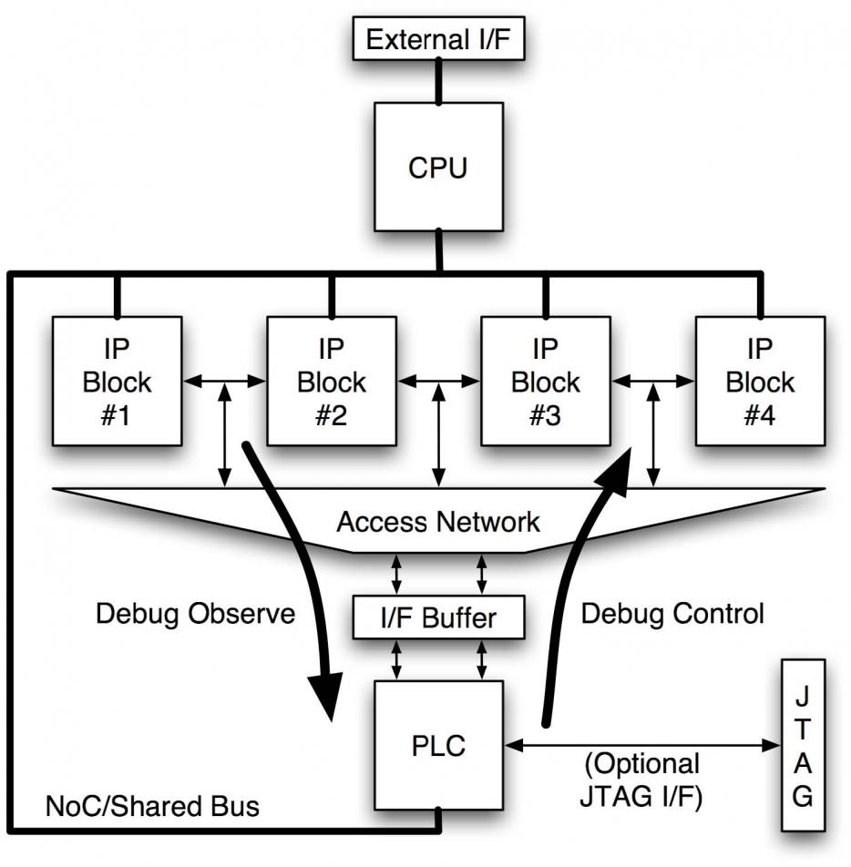
Instead of using a fixed number of conventional test points, the approach places embedded instrumentation at every signal connecting IP blocks together, and some intra-IP signals as well. Then, instead of gathering all the inputs from all the test points, a programmable interconnect allows a debugger to engage and view only the points of interest. The original diagram for this approach (which has been improved since) looks like this:

By minimizing the logic at the test point itself and implementing more generalized programmable logic to configure, interconnect, and pre-process the test points, a few things are achieved.
- Debug circuits can be implemented in existing FPGA architectures, not specialized logic.
- Centralized logic makes efficient use of expensive resources, while test points are simple.
- Circuits are flexible, not requiring things like pre-defined triggering schemes.
One might think the overhead to this approach, even in keeping the test point logic minimal, would be excessive. It turns out the typical overhead is less than 5%, and the larger a design becomes the smaller that figure gets. Subsequent improvements to these tools added the capability to tune the overhead to even smaller numbers.
To solve the issues allowing debug to run at full speed, a two-stage concentrator network design with an asynchronous implementation is employed. This obviated the need for a high-speed, low-skew clock tree that would have created problems of its own.
An understated possible benefit of this embedded instrumentation approach is error correction, or even self-healing of the SoC design may be possible. Timing closure adjustments based on large-scale visibility to signals might be performed automatically.
Quinton’s work has matured in the years following this paper, so keep in mind some specifics of the approach have changed and improved. It is a fascinating read, and I think if you explore it along with the current Tek post-silicon collateral in our Wiki, you’ll have a much better understanding of how this works inside an SoC design.
Share this post via:


Captain America: Can Elon Musk Save America’s Chip Manufacturing Industry?