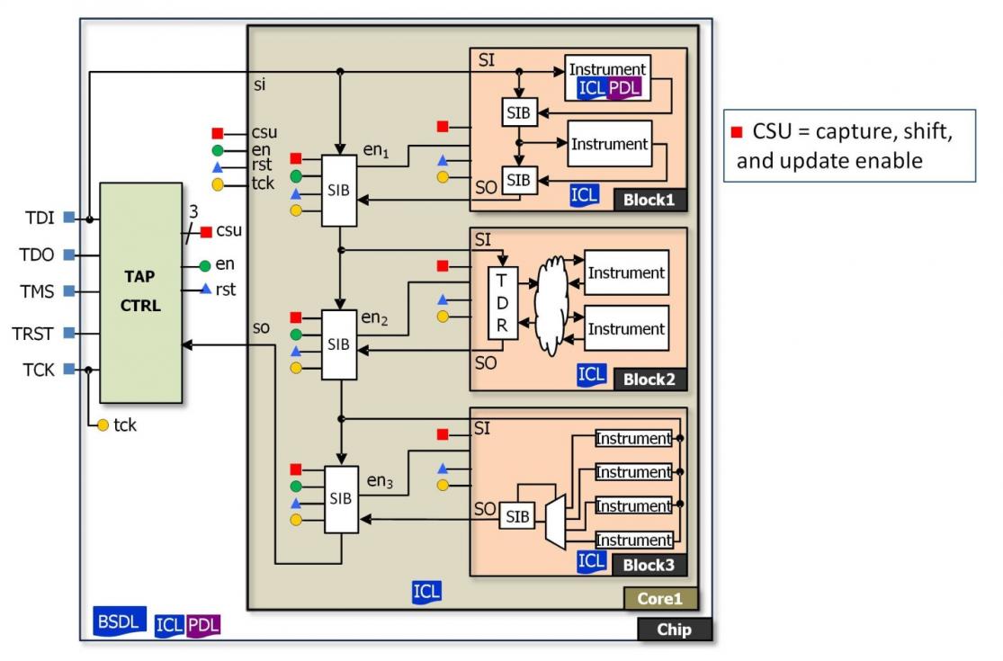
The creation of test patterns for mixed signal IP has been, to a large extent, a manual effort. To improve the process used to test, access, and control embedded IP, a new IEEE P1687 standard is being defined by a broad coalition of IP vendors, IP users, major ATE companies, and all three major EDA vendors. This new standard, also called IJTAG, is expected to be rapidly and widely adopted by the semiconductor industry. The P1687 standard will enable the industry to develop test patterns for IPs on the IP level without having to know how the IP will be embedded within different designs.

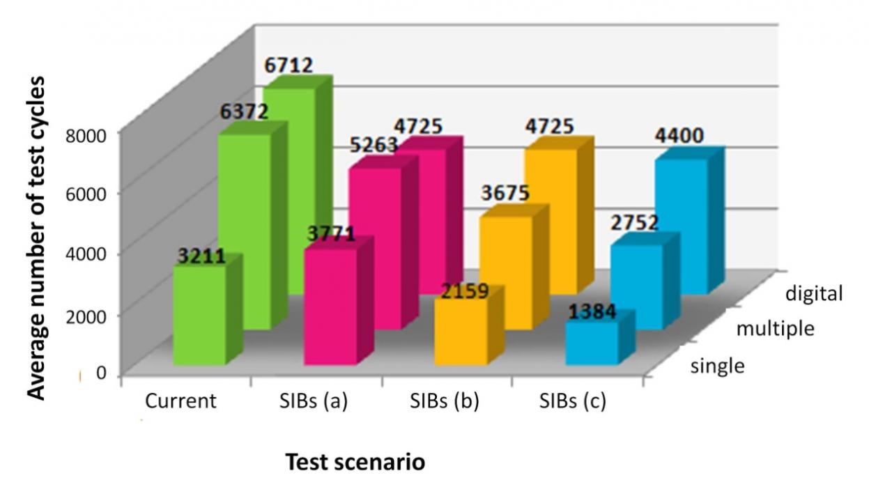
Tight co-operation between NXP and Mentor Graphics has demonstrated the benefits of using IEEE P1687 on a real industrial design manufactured at the 65 nm technology node. We created PDL files for the test setup of embedded mixed signal blocks on the instrument level. We also created the ICL descriptions of the instruments and their connections, up to the top level of the design. These experiments used Tessent IJTAG to automatically retarget the PDL descriptions from instrument level to the top-level chip pins. Top-level test benches were created to validate the correctness of the mixed signal tests. Test vectors were created as well, to transfer the test patterns to a production test. The results clearly show that test setup length can be reduced by up to 56%.
Furthermore, we confirmed that implementing the IJTAG-based tests can be done with a high level of automation. This demonstrates that tests described by IP providers at the instrument level can be automatically retargeted to the top level of the chip with a minimum of user input. Read the details in this white paper by Mentor Graphics and NXP Semiconductors.


Comments
0 Replies to “Mentor and NXP Demonstrate that IJTAG Can Reduce Test Setup Time for Complex SoCs”
You must register or log in to view/post comments.