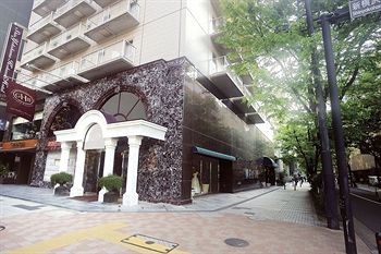
 The 1st Atrenta Technology Forum in Japan (well, it used to be the user group meeting, so it’s only the first in a very technical sense) is next week on July 19th from 1pm until 5.15pm. It will be held in the Shin-Yokohama Kokusai Hotel (how to access it here).
In the unlikely event that non-Japanese are reading this blog, here’s the story about Shin-Yokohama (“shin” means new in Japanese. And Chinese as it happens: Hsinchu). When they built the first of what people in the US call bullet trains and are prosaically called shinkansen (new line) in Japan, it was impractical to route it through Yokohama station, so they built a brand new station in the middle of rural fields outside Yokohama and that was Shin-Yokohama Station. That was in the early 1960s. Since then a whole new town, Shin-Yokohama has grown up around it.
Here is the agenda for the meeting:
- 13.00-13.30 Registration
- 13.30 to 14.00 Semiconductor market and design trends. Atrenta Japan
- 14.00 to 14.30 TSMC quality assesment with DMP 3D graphics IPcore. Digital Media Profesionals.
- 14.30 to 14.45 What’s SpyGlass Advanced Lint. Atrenta Japan.
- 14.45 to 15.15 Tips on asynchronous design and case study with SpyGlass family. Nippon System Ware Co
- 15.15 to 16.00 Break and demo
- 16.00 to 16.15 What’s SpyGlass Physical Base, Atrenta Japan.
- 16.15 to 16.30 SpyGlass Physical case study. Renasas Electronic Corporation.
- 16.30 to 16.45 Atrenta Update. Atrenta Japan.
- 16.45 to 17.15 Update for 2011 STARC Design Style Guide
For more information including how to register to attend (in Japanese) is here.
Share this post via:


Silicon Insurance: Why eFPGA is Cheaper Than a Respin — and Why It Matters in the Intel 18A Era