My first chip design at Intel was a DRAM and we had a 5% yield problem caused by electromigration issues, yes, you can have EM issues even with 6um NMOS technology. We had lots of questions but precious few answers on how to pinpoint and eliminate the source of yield loss. Fortunately, with the next generation of DRAM quickly introduced this yield issue was less urgent.

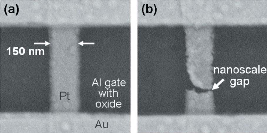
Source: Ralph Group
The DATE conference has some excellent seminars to get you up to speed on this topic and on March 14th GLOBALFOUNDRIES and Mentor have a seminar titled, Optimizing Yield and Performance in a Nanometer World. You have to register in advance to ensure a seat.

Foundries should certainly continue to push test chips through their fabs to start getting the process yield under control and help the yield ramp, monitoring and optimization.
Every design can have yield issues that are specific to that IC layout topology and stimulus being used during test. How would you go about identifying layout issues that are limiting your chip yield at 65nm and below nodes?
The good news is that cooperation between foundry and EDA companies are tight and they’ve put to together a methodology to help you. At this seminar you’ll hear how design and test failure data is used by scan test diagnosis that actually pinpoint where the defects are located and what failure mechanisms are occurring.
I was surprised to learn that the software has gotten smart enough to tell me what class the defect is part of. Statistical analysis also comes into play so that scan test diagnosis can identify systematic defects.
Geir Eide from Mentor Graphics and Thomass Herrmann from GLOBALFOUNDRIES are the presenters for this seminar.

Geir Eide, Mentor Graphics
What You Will Learn
- Best practices for data collection and diagnosis of digital semiconductor devices in a fabless/foundry flow
- Techniques to pick the correct dies for an effective failure analysis
- Layout-aware diagnosis
- Diagnosis-driven yield analysis
- DFM-aware yield analysis
- Case studies based on 32nm and 28nm silicon data
Who Should Attend
- Engineers and managers responsible for physical design, test, quality, or yield of a product
- Engineers and managers responsible for product and technology bring-up
- Failure Analysis Lab Managers or Process Engineers
- Engineers involved in manufacturing production or process development
- Anyone involved with the financial impact of low yield or low product quality


Comments
There are no comments yet.
You must register or log in to view/post comments.