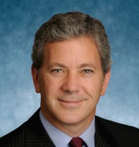
Stephen Rothrock founded ATREG in 2000 to help global advanced technology companies divest and acquire infrastructure-rich manufacturing assets. Over the last 25 years, his firm has completed more than 100 transactions, representing over 40% of all global operational wafer fab sales in the semiconductor industry for operational, warm, and cold shells. Prior to founding ATREG, Stephen established Colliers International’s Global Corporate Services initiative and headed the company’s U.S. division based in Seattle, Wash. Before that, he worked as Director for Savills International commercial real estate brokerage in London, UK, also serving on the UK-listed property company’s international board. He also spent four years near Paris, France working for an international NGO.
Tell us about how ATREG came about.
In the late 90s, Japan was heavily divesting from U.S. semiconductor manufacturing assets due to falling memory prices and the high exchange rate of the Yen against the U.S. Dollar. Having had some cleanroom experience through work I had done with AT&T in Europe, several Japanese companies approached me when I was with Colliers International asking if I could help them divest some of their wafer fabs located in the Pacific Northwest. That’s how I ended up selling two 200mm fabs, including Matsushita Puyallup, WA and Fujitsu Gresham, OR, to Microchip. Then we sold a facility for Sony down in Eugene, OR and NEC invited us to sell its 200mm facility in Scotland. After closing these fab transactions for Japanese companies, I recognized a gap in the market and decided to create a special internal division named Advanced Technology Real Estate Group (ATREG), dedicated exclusively to transactions focused on infrastructure-rich semiconductor cleanroom and manufacturing assets. We realized that if we sold a facility with an operational tool line, workforce, and an ongoing supply agreement, there would be a market for wafer fab divestment and acquisition services to other chip makers at a time when the industry was consolidating, not just in Asia, but also in the U.S. and Europe. The business took off through assignments with IBM, Infineon, Micron, and a number of Silicon Valley firms such as Maxim. Eventually, I spun the division out of Colliers International and ATREG was born.
What factors do you attribute ATREG’s success to?
After operating for 25 years, ATREG is still the only premier global firm in the world dedicated to initiating, brokering, and executing the exchange of advanced technology cleanroom manufacturing assets. ATREG has served as an objective intermediary in the transfer of over $30 billion in assets so far, acting as an indispensable conduit for the growth of its partners and the industry as a whole. There was a real need to help advanced technology companies with their global manufacturing disposition strategies because they didn’t know where to start.
As we continued to conduct fab transactions, we collected significant data on global cleanroom assets and critical deal points. Most companies didn’t have the internal staff, knowledge, or ability to allocate the time and resources necessary to execute these types of transactions. Trust and integrity were key to discussing these very sensitive issues given the financial and balance sheet effect. Over time, ATREG has built trusted relationships with many of the high-level C-suite executives in the semiconductor industry to facilitate these transactions. Our key objective is to work hand in hand with sellers and buyers alike to find the right asset strategy while simultaneously retaining as much human capital as possible when fabs change hands. CEOs call us when they need to respond to ever-changing market conditions and adjust their manufacturing strategy to reposition themselves in the global marketplace, ensure capacity, and meet customer needs.
What does your competitive landscape look like and how do you differentiate?
What ATREG offers is unique and there isn’t a firm like us anywhere else in the world. We are the go-to partner in the semiconductor industry to identify opportunities, find creative solutions, and drive competitive demand for the exchange of holistic advanced technology facilities. We facilitate the comprehensive sale and purchase of everything our clients need to be fully operational from day one – including supply agreements, human capital, tool lines, and intellectual property. We have an entrenched ability to evolve amid ever-changing global market conditions, based on 25 years of global experience. We are also very committed to human capital retention – and the significant value it adds – across all the transactions we are involved in.
What things keep your customers up at night?
The semiconductor manufacturing industry is a multifaceted, highly complex and competitive environment, subject to constant geopolitical tensions and unexpected global events (pandemics, natural disasters, etc.) Chip makers bear a lot on their shoulders. On top of having to keep up with the latest technological advances to meet ever-pressing customer demand, they need to accelerate time-to-market while keeping manufacturing costs down. The situation has worsened since the Covid pandemic, with costs and lead times spinning out of control. Add other considerations such as the labor shortage to staff greenfield fabs, protecting intellectual property, supply chain issues, sustainability compliance, or shorter product cycles, all of which impact manufacturing assets. That’s when ATREG comes in to alleviate some of that load by providing expert advice on how to address some of these strategic issues.
What are the strategic benefits of selling and buying brownfield fabs for chip makers?
On the sell side, they include fabless or fab-lite strategic initiatives, gross margin pressure, and underutilization whose root cause is often demand based. In addition, we have products coming to their end of life, CapEx requirements to continue advancing technology capabilities (there are infrastructure limitations for a site to move from 200mm to 300mm), and consolidation into other fabs, often for cleanroom shell sales. Examples include onsemi who needed to consolidate its U.S. fab portfolio to come out of low-margin businesses. Buying the East Fishkill 300mm fab gave the company 2.5 times more capacity. In Asia, Allegro MicroSystems sold a cleanroom in Thailand to consolidate all of its production to its site in the Philippines where it had extra space.
On the buy side, what makes fabs valuable is different from the driving force behind a disposition. Core reasons include geopolitical de-risking, allocation and manufacturing control, scaling geometry requirements, and product demand. Examples include Diodes and their desire for increased internal manufacturing control, Texas Instruments and scaling geometry requirements, or VIS and increased demand for products requiring additional capacity.
What are some of the most notable fab transactions that have taken place recently?
On August 31st, Bosch announced the completion of the acquisition of TSI Semiconductors’ operational 200mm fab in Roseville, CA. Following a retooling phase beginning in 2026, the company will start producing its first SiC chips on 200mm wafers. Attracting one of Europe’s largest manufacturers to U.S. soil who has only ever produced front-end chips in Germany is a massive win for the U.S. semiconductor industry as Bosch plans to invest $1.5 billion in the Roseville site over the next few years. In Europe, the German government just granted their approval for the sale of Elmos’ Dortmund fab to U.S. company Littelfuse. In June, both companies had signed a purchase agreement for a net purchase price of approximately €93 million. In both these transactions facilitated by ATREG on behalf of TSI and Elmos respectively, both buyers committed to continue to employ both fabs’ staff, saving hundreds of jobs in an already extremely tight labor market.
What is the best advice you would give U.S. chip makers to ensure a successful manufacturing strategy in 2023 and beyond?
If there was one piece of advice I could give U.S. semiconductor manufacturers to ensure capacity and supply chain resilience, it would be that they leave no stone unturned by looking at all semiconductor manufacturing options at their disposal. Greenfield fabs with support from CHIPS Act funding is one avenue, but it will take years before these new facilities yield wafers at volume. Until permit, certification, and entitlement procedures are reformed in the U.S., this will be a cumbersome process. Plus the competition for those public funds will be fierce. The other alternative to consider is brownfield. These facilities are obviously few and far between at any one time, but as chip makers who wish to go fab-light or fabless transition their production out to foundries, some operational fab assets will become available on the market all over the world and there might just be one out there that’s right for you. E.g. companies in compound semi, GaN, GaA, SiC, and MEMS want fabs and greenfield is not necessarily the answer for them because they are too long to yield.
Also Read:
CEO Interview: Dr. Tung-chieh Chen of Maxeda
CEO Interview: Koen Verhaege, CEO of Sofics
CEO Interview: Harry Peterson of Siloxit
Breker’s Maheen Hamid Believes Shared Vision Unifying Factor for Business Success
Share this post via:


Silicon Insurance: Why eFPGA is Cheaper Than a Respin — and Why It Matters in the Intel 18A Era