You are currently viewing SemiWiki as a guest which gives you limited access to the site. To view blog comments and experience other SemiWiki features you must be a registered member. Registration is fast, simple, and absolutely free so please,
join our community today!
WP_Term Object
(
    [term_id] => 14433
    [name] => X-Subscriber
    [slug] => x-subscriber
    [term_group] => 0
    [term_taxonomy_id] => 14433
    [taxonomy] => category
    [description] =>
    [parent] => 0
    [count] => 0
    [filter] => raw
    [cat_ID] => 14433
    [category_count] => 0
    [category_description] =>
    [cat_name] => X-Subscriber
    [category_nicename] => x-subscriber
    [category_parent] => 0
    [is_post] =>
)
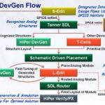
My last IC design at Intel was a Graphics Chip and I developed a layout generator for Programmable Logic Arrays (PLA) that automated the task, so I’ve always been interested in how to make IC layout more push-button and less polygon pushing. Today I watched a video about HiPer DevGen from Tanner EDA and wanted to share what I … Read More
The text of this very first article about Arteris had disapeared from Semiwiki, for an absolutely unknowed reason…If you have missed it, this is a pretty useful introduction to NoC concept, as well as to the legal battle between Arteris and Sonics:
The Network on Chip is a pretty recent concept. Let’s try to understand how … Read More
Every analog designer needs a foundry PDK (Process Design Kits) and EDA tools to design, layout and verify their AMS chip or IP. This week I had a chance to conduct an email interview with Taek-Soo Kim, VP of Technical Engineering at Dongbu HiTek in Korea. This specialty foundry supplies analog silicon worldwide.
Interview
Q: Tell… Read More
AnSem has been in the AMS design business since 1998 and uses a variety of commercial EDA tools along with internally developed tools and scripts to automate the process of analog design and technology porting. Their IC designers have completed some 40 AMS projects in diverse areas like:
- RF CMOS
- LNA, VCO, Mixers
- Synthesizers
- Low-IF/Zero-IF
…
Read More
Being an internationally recognized industry blogger (IRIB) does have its benefits, one of which is free invites to all of the cool industry conferences! The presentations are canned for the most part but you can learn a lot at the breaks and exhibits if you know the right questions to ask, which I certainly do.
The GSA Semiconductor… Read More
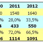
From the President: Another Great YearThanks to innovative, cost-effective technology and excellence in customer support, we’ve just ended fiscal year 2011 (on May 31st) with solid growth. Revenue was up 8%, we added 139 new customers, and we’re continuing to reach out to technology partners for MEMS and for the analog and mixed-signal… Read More
Almost every week I read about a slowing world economy, yet in EDA we have some bright spots to talk about, like Tanner EDA finishing its 24th year with an 8% increase in revenue. More details are in the press release from today.
I spoke with Greg Lebsack, President of Tanner EDA on Monday to ask about how they are growing. Greg has been… Read More
…or a global recession, but that’s not the purpose of this blog. As everybody knows, Apple is designing and selling smartphones, only. Does it mean that only smartphones are generating profit in the mobile industry? As we have seen recently in Semiwiki, Apple makes 2/3 of profit of entire mobile industry.
Let’s have a look (below)… Read More
Intro
Massimo Sivilotti, Ph.D of Tanner EDA showed me their 3D field solver in the HiPer PX extraction tool at DAC last week.
Notes
Tool Suites – schematics, layout, SPICE simulation, DRC/LVS
– HiPer PX: 3D Field solvero Layers, dielectrics,
o Finite element analysis
o Boundary element methods
o 2D mode for pattern matching… Read More
Tanner EDA at DACby Daniel Payne on 06-14-2011 at 2:40 pmCategories: EDA, Tanner EDA
Intro
For 22 years now Tanner EDAhas been in the business pf offering tools for AMS and MEMS designers. I learned what’s new at DAC on Tuesday morning.
Notes
Nicholas Williams – Director of Product Management
Tanner EDA front end: S-Edit integrates with Berkeley Fast Analog Simulator
W-Edit – is the waveform viewer
Who is … Read More