You are currently viewing SemiWiki as a guest which gives you limited access to the site. To view blog comments and experience other SemiWiki features you must be a registered member. Registration is fast, simple, and absolutely free so please,
join our community today!
            WP_Term Object
(
    [term_id] => 24
    [name] => TSMC
    [slug] => tsmc
    [term_group] => 0
    [term_taxonomy_id] => 24
    [taxonomy] => category
    [description] =>
    [parent] => 158
    [count] => 621
    [filter] => raw
    [cat_ID] => 24
    [category_count] => 621
    [category_description] =>
    [cat_name] => TSMC
    [category_nicename] => tsmc
    [category_parent] => 158
    [is_post] =>
)

WP_Term Object
(
    [term_id] => 24
    [name] => TSMC
    [slug] => tsmc
    [term_group] => 0
    [term_taxonomy_id] => 24
    [taxonomy] => category
    [description] =>
    [parent] => 158
    [count] => 621
    [filter] => raw
    [cat_ID] => 24
    [category_count] => 621
    [category_description] =>
    [cat_name] => TSMC
    [category_nicename] => tsmc
    [category_parent] => 158
    [is_post] =>
)
Synopsys made significant announcements during the recent TSMC OIP Ecosystem Forum, showcasing a range of cutting-edge solutions designed to address the growing complexities in semiconductor design. With a strong emphasis on enabling next-generation chip architectures, Synopsys introduced both new technologies and … Read More
Even though this is the 16th OIP event please remember that TSMC has been working closely with EDA and IP companies for 20+ years with reference flows and other design enablement and silicon verification activities. The father of OIP officially is Dr. Morris Chang who named it the Grand Alliance. However, Dr. Cliff Hou is the one … Read More
The 2024 live conferences have been well attended thus far and there are many more to come. The next big event in Silicon Valley is the TSMC Global OIP Ecosystem Forum on September 25th at the Santa Clara Convention Center. I expect a big crowd filled with both customers and partners.
This is the 16th year of OIP and it has been an honor… Read More
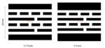
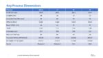
At IEDM 2019, TSMC revealed two versions of 5nm standard cell layouts: a 5.5-track DUV-patterned version and a 6-track EUV-patterned version [1]. Although the metal pitches were not explicitly stated, later analyses of a 5nm product, namely, Apple’s A15 Bionic chip, revealed a cell height of 210 nm [2]. For the 6-track … Read More
When Intel entered the foundry business with IDM 2.0 I was impressed. Yes, Intel had tried the foundry business before but this time they changed the face of the company with IDM 2.0 and went “all-in” so to speak. The progress has been impressive and today I think Intel is well positioned to capture the NOT TSMC business by providing… Read More
At the VLSI Technology Symposium this week Intel released details on their i3 process. Over the last four nodes Intel has had an interesting process progression. In 2019, 10nm finally entered production with both high performance and high-density standard cells. 10nm went through several iterations eventually resulting in… Read More
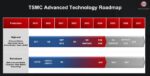
The TSMC Technology Symposium provides a worldwide stage for TSMC to showcase its advanced technology impact and the extensive ecosystem that is part of the company’s vast reach. These events occur around the world and the schedule is winding down. TSMC covers many topics at its Technology Symposium, including industry-leading… Read More
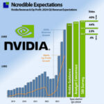
This article previews Nvidia’s earnings release and will be updated during and after the earnings release. As usual, we will compare and contrast the Nvidia earnings with our supply chain glasses to identify changes and derive insights. Please return to this article, as it will be updated over the next week as we progress with our… Read More
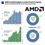
AMD’s Q1-2024 financial results are out, prompting us to delve into the Data Center Processing market. This analysis, usually reserved for us Semiconductor aficionados, has taken on a new dimension. The rise of AI products, now the gold standard for semiconductor companies, has sparked a revolution in the industry, making… Read More
NVIDIA cuLitho Accelerates Semiconductor Manufacturing’s Most Compute-Intensive Workload by 40-60x, Opens Industry to New Generative AI Algorithms.
An incredible example of semiconductor industry partnerships was revealed during the Synopsys User Group (SNUG) last month. It started with a press release but there is much… Read More