You are currently viewing SemiWiki as a guest which gives you limited access to the site. To view blog comments and experience other SemiWiki features you must be a registered member. Registration is fast, simple, and absolutely free so please,
join our community today!
            WP_Term Object
(
    [term_id] => 14
    [name] => Synopsys
    [slug] => synopsys
    [term_group] => 0
    [term_taxonomy_id] => 14
    [taxonomy] => category
    [description] =>
    [parent] => 157
    [count] => 784
    [filter] => raw
    [cat_ID] => 14
    [category_count] => 784
    [category_description] =>
    [cat_name] => Synopsys
    [category_nicename] => synopsys
    [category_parent] => 157
    [is_post] =>
)

WP_Term Object
(
    [term_id] => 14
    [name] => Synopsys
    [slug] => synopsys
    [term_group] => 0
    [term_taxonomy_id] => 14
    [taxonomy] => category
    [description] =>
    [parent] => 157
    [count] => 784
    [filter] => raw
    [cat_ID] => 14
    [category_count] => 784
    [category_description] =>
    [cat_name] => Synopsys
    [category_nicename] => synopsys
    [category_parent] => 157
    [is_post] =>
)
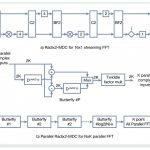
A basic building block of any communication system today is the fast Fourier transform, or FFT. A big advantage of FPGA implementations of FFTs is they can be scaled and tuned for the task at hand, optimizing data flow, resource use, and power consumption. Scaled, that is, up to the clock speed of the FPGA – or so it would seem.
Today’s… Read More
I met Mike Sanie around DVCon time and planned to write a blog about the one year anniversary of Synopsys Discovery VIP which was announced during Aart’s keynote at DVCon in 2012. Eric covered it for SemiWiki here. But Synopsys had other stuff they wanted me to blog about and so it is a couple of months late. The 14th month anniversary… Read More
… is now 8 years old, and the money paid for this 10 engineers start-up was considered, at that time, as a “bingo” for Cascade’s funders: “In October 2004, the Company completed the acquisition of Cascade Semiconductor Solutions, Inc. (Cascade) for total upfront consideration of $15.8 million and contingent consideration of … Read More
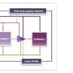
The burgeoning need of high density of electronic content on a single chip, thereby necessitating critical PPA (Power, Performance, Area) optimization, has pushed the technology node below 0.1 micron where static power becomes equally relevant as dynamic power. Moreover, multiple power rails run through the circuit at different… Read More
Cliff Hou of TSMC gave the keynote today at SNUG on Collaborate to Innovate: a Foundry’s Perspective. Starting around 45nm the way that a foundry has to work with its ecosystem fundamentally changed. Up until then, each process generation was similar enough to the previous one, apart obviously from size, that it could be … Read More
Will 14nm Yield?by Daniel Nenni on 03-26-2013 at 9:00 pmCategories: EDA, Synopsys
If I had a nickel for every time I heard the term “FinFET” at the 2013 SNUG (Synopsys User Group) Conference I could buy a dozen Venti Carmel Frappuccinos at Starbucks (my daughter’s favorite treat). In the keynote, Aart de Geus said FinFET 14 times and posed the question: Will FinFETs Yield at 14nm? So that was my mission, ask everybody… Read More
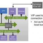
So, you dropped that piece of complex IP you just licensed into an SoC design, and now it is time to fire up the simulator. How do you verify that it actually works in your design? If you didn’t get verification IP (VIP) with the functional IP, it might be a really long day.
Compliance checking something like a PCIe interface block is a … Read More
I was at SNUG earlier today at both Aart’s keynote that opened the conference and at his “meet the press” Q&A just before lunch. The keynote was entitled Bridges to the Gigascale Decade. And the presentation certainly contained lots of photos of bridges! Anyway, I’m going to focus on just one thing,… Read More
Pure digital routers for IC designs have an easier task than mixed-signal routers, because mixed-signal routers have more constraints like:
- Shielded buses
- Differential pairs
- Twisted pairs
- Matched RC routing
- 20nm technology rules
- Double Patterning Technology (DPT)
…
Read More
Yesterday evening was the annual EDAC CEO forecast meeting. Actually it is not really a forecast meeting any more, more a sort of CEO response to some survey questions asked of EDAC members. Rich Valera of Needham moderated with Lip-Bu, Aart and Wally, along with Simon Segars representing the IP arm(!) of the business and Raul Camposano… Read More