You are currently viewing SemiWiki as a guest which gives you limited access to the site. To view blog comments and experience other SemiWiki features you must be a registered member. Registration is fast, simple, and absolutely free so please,
join our community today!
WP_Term Object
(
    [term_id] => 386
    [name] => Semiconductor Services
    [slug] => semiconductor-services
    [term_group] => 0
    [term_taxonomy_id] => 386
    [taxonomy] => category
    [description] =>
    [parent] => 0
    [count] => 1195
    [filter] => raw
    [cat_ID] => 386
    [category_count] => 1195
    [category_description] =>
    [cat_name] => Semiconductor Services
    [category_nicename] => semiconductor-services
    [category_parent] => 0
    [is_post] =>
)
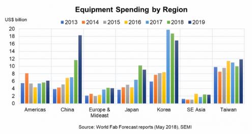
We attended Semicon West Monday and Tuesday, the annual show for the semi equipment industry. Its very clear from discussions with all our sources in the industry that confirm that Samsung has put the brakes on spending on memory and that message was reinforced by declines in their expected profitability due to weaker memory pricing.… Read More
Welcome to my newly relocated column, I am so excited about my new relationship with Daniel Nenni, and the other esteemed bloggers on SemiWiki. For those who do not know me, I have been a featured columnist on another EDA portal for the past 12-plus years, and in EDA for 20-plus years. As the leading recruiter in our industry, (or so … Read More
You’re excited about the business potential for your cool new baby monitor, geo-fenced kid’s watch, home security system or whatever breakthrough app you want to build. You want to focus on the capabilities of the system, connecting it to the cloud and your marketing rollout plan. Then someone asks whether your system is architected… Read More
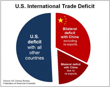
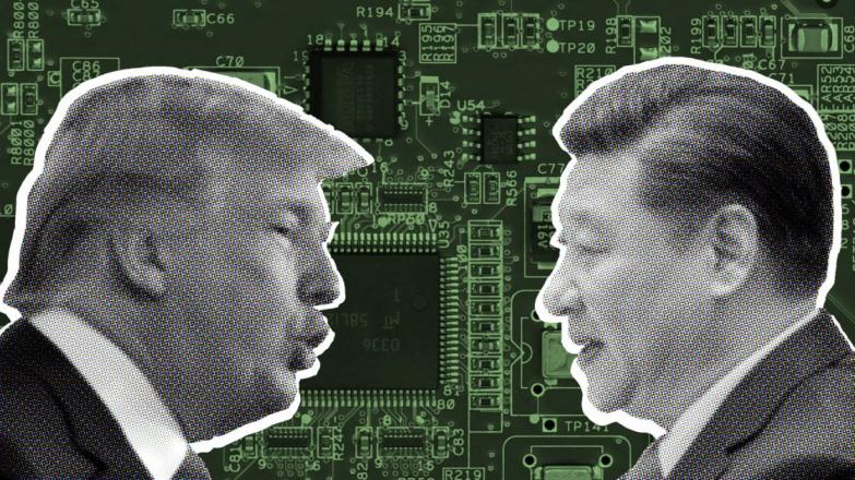
China didn’t wait around for the US to announce more tariffs or export restrictions, instead it went on the offensive and put an injunction in place to prevent Micron from shipping product into China. Although our view is that Micron will see little impact from this action, the headlines caused the semiconductor sector stocks… Read More
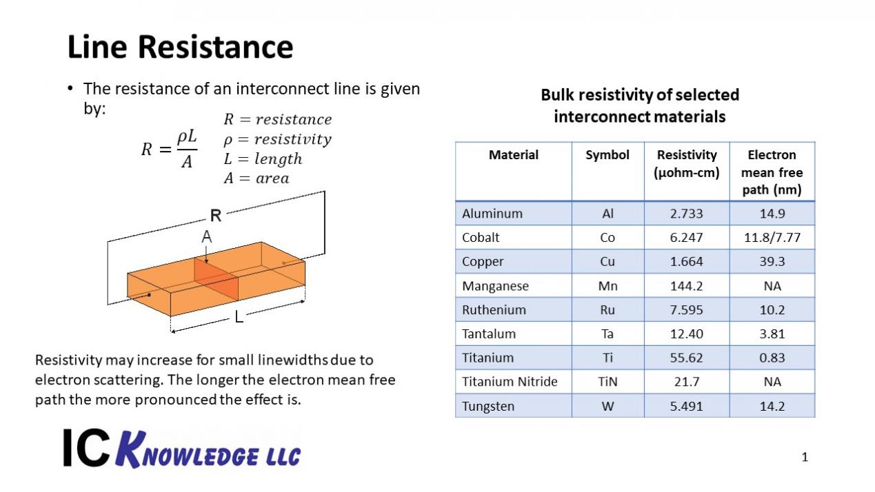
The IEEE Interconnect Technology Conference (IITC): Advanced Metallization Conference was held June 4th through 7th in Santa Clara. Imec presented multiple papers on comparing copper, cobalt and ruthenium interconnect. One paper in particular caught my eye: Marleen H. van der Veen, # N. Heylen, O. Varela Pedreira, S. Decoster,… Read More
As we have been warning for months the China trade issue continues to grow and accelerate. As we are approaching the June 30th cliff (when export sanctions will be announced) it seems as if the administration has given the industry a kick so we fly even further. The US will also restrict Chinese investment in US tech companies. The … Read More
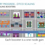
At the Imec technology forum in Belgium, Dan Mocuta and Juliana Radu presented “Evolution and Disruption: A Perspective on Logic Scaling and Beyond”, I also had a chance to sit down with Dan and discuss the presentation.
Device scaling
Scaling of devices will only get you so far, you need to look at new devices and new… Read More
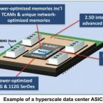
We all know IP is critical for advanced ASIC design. Well-designed and carefully tested IP blocks and subsystems are the lifeblood of any advanced chip project. Those IP suppliers who can measure up to the need, especially at advanced process nodes, will do well, absolutely.
It is interesting to note that eSilicon now has a very … Read More
It appears the current cycle has rolled over? The reason is memory & could be worsened by trade Figuring out length, depth and impact of the downturn? We had said that AMAT “called” the top of the cycle on their last conference call even though they may not think so. Semiconductor cycles always ends the same way. The… Read More
If you read around topics in advanced formal verification you’re likely to run into something called Wolper coloring, or what Vigyan Singhal (Chief Oski at Oski) calls the Wolper method. Many domains have specialized techniques but what’s surprising in this instance is a seeming absence of helpful on-line explanations (though… Read More


Intel, Musk, and the Tweet That Launched a 1000 Ships on a Becalmed Sea