In fact, this is the title of a presentation given by Pete Foley during FD-SOI Forum 2014 held in Shanghai, a couple of weeks ago. What is nice with clever people like Pete Foley is that they get the point, and get it quickly. Getting the point is to insert AND in capital in the title, as using FD-SOI technology allows to benefit from low-power… Read More

Intel Invades China Mobile Market!
As you may have heard, Intel is making some interesting moves into the China mobile market. At first it had me a bit puzzled but I had some lengthy discussions about it during ARM TechCon last week so I’m ready to start writing. Spoiler alert: This will be pro Intel so please sit down and take some deep breaths before reading.
The first… Read More
The Apple Samsung TSMC Intel 14nm Mashup!
One of the strengths of the fabless semiconductor ecosystem is competition since it keeps innovation high and prices low. One of the challenges of fostering competition is that you have to make good on a threat of using a competing product during a pricing negotiation. Well, in my opinion, for the next version of the iPhone, Apple… Read More
Key Collaboration to Enable Designs at Advanced Nodes
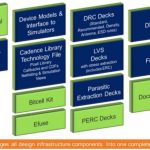
In the semiconductor ecosystem, several partners (or better to say stakeholders) join together in the overall value chain to finally output the most coveted chip, err I should say SoC these days. It becomes really interesting when we start analyzing the real value added by each of them, none appears to be less. Well, then to whom … Read More
GlobalFoundries and Samsung at ARM
It was back in April that GlobalFoundries and Samsung announced that GF would license Samsung’s 14nm process to run in their Fab8 in upstate New York. Since then there has not really been any news and of course those of us that follow the foundry industry wondered to what extent there was real substance to the agreement or if … Read More
A de-parallel universe for Windows 10
It was CES 2011 when Steve Ballmer sweatered up and pitched the coming universe according to Microsoft, where the same Windows base would run on everything – PC, phone, tablet, and game console. Getting from that visionary statement to Windows 10 hasn’t been a smooth ride.… Read More
ARM ♥ TSMC!
This week is the 10[SUP]th[/SUP] annual ARM Technical Conference in Silicon Valley. In regards to size, content, and relevance, I believe ARM TechCon is the #1 event for the fabless semiconductor ecosystem for sure. I attended keynotes, sessions, and walked the hallways on Wednesday and Thursday. I wish I could write about everything… Read More
Semiconductor double digit growth in 2014 & 2015
The global semiconductor market was US$82.2 billion in the second quarter of 2014 according to World Semiconductor Trade Statistics (WSTS). 2Q 2014 was up 4.8% from 1Q 2014 up 10.1% from 2Q 2013. Healthy growth should continue into 3Q 2014. The table below shows initial revenue growth guidance for 2Q 2014, final reported revenue… Read More
Cortex-M7: 6-stage, cached, 400 MHz MCU
“Who needs a 32-bit MCU?” It was a question asked a million times in the press when ARM introduced the Cortex-M family back in 2004. In fairness, that question predates the Internet of Things, with wireless sensor networks, open source code, encryption, and more needs for connected devices.… Read More
Who Will Lead at 10nm?
There has been a lot of discussion on SemiWiki lately around 14nm FinFET technology and who really leads and by how much. I thought it would be interesting to review some process metrics for previous technology generation and then make some forecasts around 10nm.
The focus of this article will be Intel, TSMC and Global Foundries/Samsung… Read More
Enhancing Multi-Domain System Simulation with FMI Co-Simulation