You are currently viewing SemiWiki as a guest which gives you limited access to the site. To view blog comments and experience other SemiWiki features you must be a registered member. Registration is fast, simple, and absolutely free so please,
join our community today!
WP_Term Object
(
    [term_id] => 16126
    [name] => Lithography
    [slug] => lithography
    [term_group] => 0
    [term_taxonomy_id] => 16126
    [taxonomy] => category
    [description] =>
    [parent] => 0
    [count] => 190
    [filter] => raw
    [cat_ID] => 16126
    [category_count] => 190
    [category_description] =>
    [cat_name] => Lithography
    [category_nicename] => lithography
    [category_parent] => 0
    [is_post] =>
)
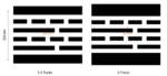
At IEDM 2019, TSMC revealed two versions of 5nm standard cell layouts: a 5.5-track DUV-patterned version and a 6-track EUV-patterned version [1]. Although the metal pitches were not explicitly stated, later analyses of a 5nm product, namely, Apple’s A15 Bionic chip, revealed a cell height of 210 nm [2]. For the 6-track … Read More
The latest significant development in EUV lithography technology is the arrival of High-NA systems. Theoretically, by increasing the numerical aperture, or NA, from 0.33 to 0.55, the absolute minimum half-pitch is reduced by 40%, from 10 nm to 6 nm. However, for EUV systems, we need to recognize that the EUV light (consisting … Read More
On Friday April 12th Intel held a press briefing on their adoption of High NA EUV with Intel fellow and director of lithography Mark Phillips.
In 1976 Intel built Fab 4 in Oregon, the first Intel fab outside of California. With the introduction of 300mm Oregon became the only development site for Intel with large manufacturing, development,… Read More
There has been much interest in Huawei’s and SMIC’s plans for 5nm production in the near future. Since there is no use of EUV in China, immersion DUV lithography (with a 76 nm pitch resolution) is expected to be used along with pitch quartering to achieve pitches in the 20-30 nm range expected for the 5nm and 3nm nodes [1].… Read More
ASML- better EPS but weaker revenues- 2024 recovery on track
China jumps 10% to 49%- Memory looking better @59% of orders
Order lumpiness increases with ASP- EUV will be up-DUV down
“Passing Bottom” of what has been a long down cycle
Weak revenues & orders but OK EPS
Reported revenue was Euro5.3B and EPS of Euro3.11… Read More
NVIDIA cuLitho Accelerates Semiconductor Manufacturing’s Most Compute-Intensive Workload by 40-60x, Opens Industry to New Generative AI Algorithms.
An incredible example of semiconductor industry partnerships was revealed during the Synopsys User Group (SNUG) last month. It started with a press release but there is much… Read More
Resist blur remains a topic that is relatively unexplored in lithography. Blur has the effect of reducing the difference between the maximum and minimum doses in the local region containing the feature. Blur is particularly important for EUV lithography since EUV lithography is prone to stochastic fluctuations and also driven… Read More
The majority of EUV production is on 5nm and 3nm node, implemented by late 2022. Metal oxide resists have not been brought into volume production yet [1,2], meaning that only organic chemically amplified resists (CARs) have been used instead until now. These resists have a typical absorption coefficient of 5/um [3,4], which means
…
Read More
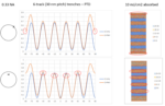
The discussion of any particular lithographic application often refers to imaging a single pitch, e.g., 30 nm pitch for a 5nm-family track metal scenario. However, it is always necessary to confirm the selected patterning techniques on the actual use case. The 7nm, 5nm, or 3nm 6-track cell has four minimum pitch tracks, flanked… Read More
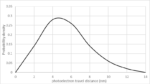
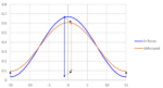
EUV lithography is a complicated process with many factors affecting the production of the final image. The EUV light itself doesn’t directly generate the images, but acts through secondary electrons which are released as a result of ionization by incoming EUV photons. Consequently, we need to be aware of the fluctuations… Read More


Enhancing Multi-Domain System Simulation with FMI Co-Simulation