So what comes after FinFETs? At 14/16nm (or 22nm if you are Intel) we had FinFET transistors, where the channel was no longer planar but stuck out of the wafer vertically, and the gate wrapped around it on 3 sides. The key thing that made FinFET transistors attractive was that the channel was thin so that the gate controlled it well. … Read More

Altera vs Xilinx FinFET Update
One of the things I do in my spare time is listen to quarterly conference calls and try to sort fact from fiction. I compare past calls to the current one and attempt to predict what’s coming next. Confucius said, “Study the past if you would define the future” and I’m a big believer in that.
Paul McLellan wrote about the Xilinx call earlier… Read More
FinFET Based Designs Made Easy & Reliable
Although semiconductor manufacturing has taken off with FinFET based process technology which provides lucrative payoffs on performance improvement, power reduction and area saving in devices for high density and high performance SoC demand of modern era, apprehensions remain about its reliability due to reduced noise … Read More
Xilinx’s 16nm vs. Altera 14nm
You will not believe this, but the family was picking me up Friday evening from the airport and on the way home… Get this, for real, the wife asks me to cut her hair tomorrow. Now the three of you that read my stuff, know what happened before. I resisted, and firmly said ‘No’…The wife seeing my macho stance began appealing to my engineer’s… Read More
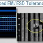
IC Power Noise Reliability for FinFET Designs

Reliability for ICs is a big deal because the last thing that you want to do is ship a new part only to find out later in the field that there are failures not being caught by testing. I’ve already had two consumer products fail this year because of probable reliability issues: My MacBook Pro with 16GB of RAM started rebooting caused… Read More
The Infamous Intel FPGA Slide!
As I have mentioned before, I’m part of the Coleman Research Group so you can rent me by the hour to better understand the semiconductor industry. Most of the conversations are by phone but sometimes I do travel to the East Coast, Taiwan, Hong Kong, and China for face-to-face meetings. Generally the calls are the result of an event … Read More
The Alternative to FinFET: FD-SOI
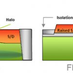
Everywhere you turn these days you find FinFETs. Intel has had them since 22nm (they use the word Tri-gate but it is the same as what the world calls FinFET) and TSMC will have them at 16nm. So why FinFET? And is there an alternative?
The reason that regular bulk planar transistors have run out of steam is that the channel area underneath… Read More
Deploying 14nm FinFETs in your Next Mobile SoC

At DAC in Austin a design company, foundry and EDA vendor teamed up to present their experiences with 14nm FinFETs during a breakfast on Tuesday.
Panelists included:
- Ed Sperling, Semi Mfg and Design
- Anil Jain, Cavium
- Subramani Kengeri, GLOBALFOUNDRIES
- Kelvin Low, GLOBALFOUNDRIES
- Raymond Leung, Synopsys
- Bari Biswas, Synopsys
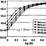
FinFET Modeling and Extraction at 16-nm

In 2012 FinFET is one of the most talked about MOS technologies of the year because traditional planar CMOS has slowed down on scaling below the 28nm node. To learn more about FinFET process modeling I attended a Synopsys webinar where Bari Biswas presented for about 42 minutes include a Q&A portion at the end.
Bari Biswas, Synopsys… Read More
Introduction to FinFET Technology Part III
The preceding two Semiwiki articles in this thread provided an overview to the FinFET structure and fabrication. The next three articles will discuss some of the unique modeling requirements and design constraints that FinFET’s introduce, compared to planar FET technology.
Due to the complexity of FinFET modeling – … Read More
Consolidation and Competition: Who is Winning the $4.5 Billion Interface IP Race?