You are currently viewing SemiWiki as a guest which gives you limited access to the site. To view blog comments and experience other SemiWiki features you must be a registered member. Registration is fast, simple, and absolutely free so please,
join our community today!
WP_Term Object
(
    [term_id] => 50
    [name] => Events
    [slug] => events
    [term_group] => 0
    [term_taxonomy_id] => 50
    [taxonomy] => category
    [description] =>
    [parent] => 0
    [count] => 1565
    [filter] => raw
    [cat_ID] => 50
    [category_count] => 1565
    [category_description] =>
    [cat_name] => Events
    [category_nicename] => events
    [category_parent] => 0
    [is_post] =>
)
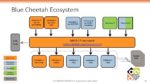
Since the start of PROMS, PLDs and FPGAs we have learned the importance of programmability in modern semiconductor design. Today we have eFPGAs for “design adaptive” embedded programmability and that is what this webinar is all about.
Several key points are discussed starting with the Law of Accelerating Returns as it applies… Read More
GlobalFoundries is one of the more interesting semiconductor stories of this decade. They started as a spinout of the AMD fabs then acquired Chartered Semiconductor Manufacturing in 2009 and the IBM Microelectronics business in 2014.
Now that events are virtual it is a great time for my fellow semiconductor professionals to
…
Read More
The 2020 VLSI Technology Symposium was held as a virtual conference from June 14th through June 19th. At the symposium Imec gave an interesting paper on Monolithic CFET and I had a chance to interview one of the authors, Hiroaki Arimura.
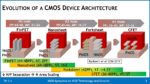
It is well known in the industry that FinFETs (FF) are reaching the end of their scaling life. Samsung… Read More
Veriest is headquartered in Israel with engineering sites in Serbia & Hungary. The team has accumulated a wealth of experience through involvement in projects in the forefront of semiconductor technology.
Veriest maintains unrivaled quality standards in terms of both service and knowledge. With the ability to take on … Read More
This is another installment covering TSMC’s very popular Open Innovation Platform event (OIP), held on August 25. This event presents a diverse and high-impact series of presentations describing how TSMC’s vast ecosystem collaborates with each other and with TSMC. The talk covered here focuses on a complete on-die clock … Read More
Recently, TSMC held their 26th annual Technology Symposium, which was conducted virtually for the first time. This article is the last of three that attempts to summarize the highlights of the presentations. This article focuses on the technology design enablement roadmap, as described by Cliff Hou, SVP, R&D.
Key Takeaways… Read More
There are many reasons today for dividing up large monolithic SoCs into chiplets that are connected together inside a single package. Let’s look at just some of these reasons. Many SoCs share a common processing core with application specific interfaces and specialized processing engines. Using chiplets would mean that it is… Read More
TSMC held their very popular Open Innovation Platform event (OIP) on August 25. The event was virtual of course and was packed with great presentations from TSMC’s vast ecosystem. One very interesting and relevant presentation was from Dolphin Design, discussing the delivery of high-performance audio processing using TSMC’s… Read More
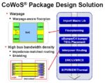
Recently, TSMC held their 26th annual Technology Symposium, which was conducted virtually for the first time. This article is the second of three that attempts to summarize the highlights of the presentations. This article focuses on the TSMC advanced packaging technology roadmap, as described by Doug Yu, VP, R&D.
Key… Read More
Designers spend plenty of time analyzing the effects of process, voltage and temperature. But everyone knows it’s not enough to simply stop there. Operating environments are tough and have lots of limitations, especially when it comes to power consumption and thermal issues. Thermal protection and even over-voltage protections… Read More


Enhancing Multi-Domain System Simulation with FMI Co-Simulation