As embedded systems continue to become more complex and integrate greater functionality, SoC developers are faced with the challenge of developing more powerful, yet more energy-efficient devices. The processors used in these embedded applications must be efficient to deliver high levels of performance within limited power… Read More

WEBINAR: Design and Verify State-of-the-Art RFICs using Synopsys / Ansys Custom Design Flow
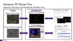
The design and characterization of RF circuits is a complex process that requires an RF designer to overcome a variety of challenges. Not only do they face the complexities posed by advanced semiconductor processes and the need to meet the demanding requirements of modern wireless standards, designers must also account for electromagnetic… Read More
DSP IP for High Performance Sensor Fusion on an Embedded Budget
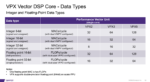
Whether we realize it or not, everyday applications we use depend on data gathered by sensors. We can bet that pretty much every application uses at least a couple of different types of sensors, if not more. That is because different types of sensors are better suited to collect data depending on the application, the environment … Read More
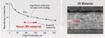
SEMICON West 2022 and the Imec Roadmap
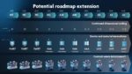
SEMICON West 2022 was held from July 12th to 14th at the Moscone Center in San Francisco.
On Monday the 11th before the show, Imec held a technology forum at the Marriott Marquee right around the corner from the Moscone center. In recent years the Imec forums have shifted away from the process technology I cover to more of a system and… Read More
The Turn of Moore’s Law from Space to Time

“It’s time for the big ship of Moore’s Law to make a turn from space to time” is a nonconformist message that surprised me when I read the book “The Turn of Moore’s Law from Space to Time” by Mr. Liming Xiu.
As a forty-year veteran and as an author of several books on the semiconductor industry myself, I am quite familiar with all contemporary… Read More
Calibre, Google and AMD Talk about Surge Compute at #59DAC
In 2022 using the cloud for EDA tasks is a popular topic, and at DAC this year I could see a bigger presence from the cloud hardware vendors in the exhibit area, along with a growing stampede of EDA companies. Tuesday at DAC there was a luncheon with experts from Siemens EDA, Google and AMD talking about surge compute. I already knew Michael… Read More
Future Semiconductor Technology Innovations
At the recent VLSI Symposium on Technology and Circuits, Dr. Y.J. Mii, Senior Vice President of Research and Development at TSMC, gave a plenary talk entitled, “Semiconductor Innovations, from Device to System”. The presentation offered insights into TSMC’s future R&D initiatives, beyond the current roadmap. The associated… Read More
Solve Embedded Development Challenges With IP-Centric Planning
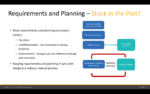
At least once if not more, many of us may have faced the following situation. We download the latest software driver for a device only to find out after installing that it doesn’t work for your hardware. As per the release notes, it should work for your hardware but in reality it does not. We have no choice but to revert back to the earlier… Read More
Clocking for High-Speed SerDes
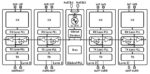
The incessant demand for faster data rates across a wide range of end applications has led to the development of the most recent generation of SerDes hardware, achieving 112Gbps. For example, network switches in datacenter architectures are starting to provide 51T throughput utilizing these new 112Gbps implementations (51.2Tbps… Read More
IEDM 2022 is shaping up
IEDM is one of the premiere conferences for the latest information on leading edge semiconductor technology. The 68th annual International Electron Devices Meeting will be held December 3rd through 7th at the San Francisco Hilton.
The paper submission deadline is July 14, 2022, and the late-news deadline is August 22, 2022. … Read More
Musk’s Orbital Compute Vision: TERAFAB and the End of the Terrestrial Data Center