TSMC covered their specialty technologies in great detail. Specialty is what we inside the ecosystem used to call weird stuff meaning non-mainstream and fairly difficult to do on leading edge processes. Specialty technologies will play an even more important part of semiconductor design with the advent of chiplets where die… Read More

TSMC 2023 North America Technology Symposium Overview Part 3
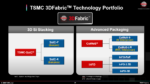
TSMC’s 3DFabric initiative was a big focus at the symposium, as it should be. I remember when TSMC first went public with CoWos the semiconductor ecosystem, including yours truly, let out a collective sigh wondering why TSMC is venturing into the comparatively low margin world of packaging. Now we know why and it is absolutely… Read More
TSMC 2023 North America Technology Symposium Overview Part 2

The next topic I would like to cover is an update to the TSMC process node roadmap starting with N3. As predicted, N3 will be the most successful node in the TSMC FinFET family. The first version of N3 went into production at the end of last year (Apple) and will roll out with other customers in 2023. There is a reported record amount of … Read More
TSMC 2023 North America Technology Symposium Overview Part 1

The TSMC 2023 North America Technology Symposium happened today so I wanted to start writing about it as there is a lot to cover. I will do summaries and other bloggers will do more in-depth coverage on the technology side in the coming weeks. Having worked in the fabless semiconductor ecosystem the majority of my 40 year semiconductor… Read More
Multi-Die Systems: The Biggest Disruption in Computing for Years

At the recent Synopsys Users Group Meeting (SNUG) I had the honor of leading a panel of experts on the topic of chiplets. The discussion was based on a report published by the MIT Technology Review Insights in cooperation with Synopsys. This is a very comprehensive report (12 pages) that is available online HERE.
Here is the preface… Read More
Taking the Risk out of Developing Your Own RISC-V Processor with Fast, Architecture-Driven, PPA Optimization

Are you developing or thinking about developing your own RISC-V processor? You’re not alone. The use of the RISC-V ISA to develop processors for SoCs is a growing trend. RISC-V offers a lot of flexibility with the ability to customize or create ISA and microarchitectural extensions to differentiate your design no matter your application… Read More
LIVE WEBINAR – The ROI of User Experience Design: Increase Sales and Minimize Costs

The semiconductor industry has seen a significant shift towards vertical integration of products, expanding from chips to generalized or purpose-built integrated solutions. As software becomes an increasingly critical component of these solutions, leveraging modern software development processes with User Experience… Read More
WEBINAR: Design Cost Reduction – How to track and predict server resources for complex chip design project?
During the design of complex chips, cost reduction is becoming a real challenge for small, medium and large companies. Resource management is a key to contain design cost.
The chip design market is expecting automated solutions to help in the resource prediction, planning and analysis. AI-based technologies are promising … Read More
LIVE WEBINAR: New Standards for Semiconductor Materials

This is the 5th webinar in our series of webinars to explore trending topics on materials and semiconductor development. Join us to discover how digital solutions are forming new ways of operating in a fast-paced, highly demanding semiconductor industry.
With data analytics and digital tools, we are setting new standards for
Full-Stack, AI-driven EDA Suite for Chipmakers

Semiconductor technology is among the most complex of technologies and the semiconductor industry is among the most demanding of industries. Yet the ecosystem has delivered incredible advances over the last six decades from which the world has benefitted tremendously. Yes, of course, the markets want that break-neck speed… Read More
Intel, Musk, and the Tweet That Launched a 1000 Ships on a Becalmed Sea