You are currently viewing SemiWiki as a guest which gives you limited access to the site. To view blog comments and experience other SemiWiki features you must be a registered member. Registration is fast, simple, and absolutely free so please,
join our community today!
            WP_Term Object
(
    [term_id] => 159
    [name] => Siemens EDA
    [slug] => siemens-eda
    [term_group] => 0
    [term_taxonomy_id] => 159
    [taxonomy] => category
    [description] =>
    [parent] => 157
    [count] => 841
    [filter] => raw
    [cat_ID] => 159
    [category_count] => 841
    [category_description] =>
    [cat_name] => Siemens EDA
    [category_nicename] => siemens-eda
    [category_parent] => 157
    [is_post] =>
)

WP_Term Object
(
    [term_id] => 159
    [name] => Siemens EDA
    [slug] => siemens-eda
    [term_group] => 0
    [term_taxonomy_id] => 159
    [taxonomy] => category
    [description] =>
    [parent] => 157
    [count] => 841
    [filter] => raw
    [cat_ID] => 159
    [category_count] => 841
    [category_description] =>
    [cat_name] => Siemens EDA
    [category_nicename] => siemens-eda
    [category_parent] => 157
    [is_post] =>
)
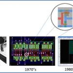
Have you seen the latest design rule manuals? At 28nm and 20nm design sign-off is no longer just DRC and LVS. These basic components of physical verification are being augmented by an expansive set of yield analysis and critical feature identification capabilities, as well as layout enhancements, printability, and performance… Read More
If verification is the art of determining that your design works correctly under all specified conditions, then it is imperative that we are able to create an environment that can tell you if this is truly the case.
Scoreboards are verification components that determine that the DUT is working correctly, including ensuring that… Read More
If you are involved in testing memory or logic of ARM-based designs, you’ll want to attend this free seminar on July 17, 2012 in Santa Clara. Mentor Graphics and ARM have a long standing partnership, and have optimized the Mentor test products (a.k.a Tessent) for the ARM processors and memory IP.
The lunch seminar runs from 10:30-1:00… Read More
IC Test Sessions at SEMICON West 2012by Beth Martin on 07-02-2012 at 1:43 pmCategories: EDA, Siemens EDA
SEMICON West is coming up this July 10-12 at the Moscone Center in San Francisco. It covers a broad swath of the microelectronics supply chain, but I was particularly interested in the test sessions. Here are two that I recommend.
“The Value of Test for Semiconductor Yield Learning” on Tuesday, July 10, at 1:30p. The… Read More
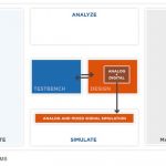
I met with Jay Madiraju of Mentor Graphics on Wednesday at DAC to get an update on their AMS simulation products. We worked together at Mentor back when Mach TA was being developed as a Fast SPICE circuit simulator.… Read More
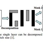
David Abercrombie from Mentor Graphics met with me on Tuesday at DAC to provide an update on DPT – Double Patterning Technology, something new required for several layers starting at the 20nm node in order to get any IC yield. DPT is also part of Multiple-Patterning.… Read More
The days following a major conference like DAC are a good time to reflect on the overall health and vibrancy of the electronic design automation (EDA) industry. I’ve been in EDA for 21 years and built two successful startups, and over the last couple of years, have witnessed some decline in both new talent and in venture investment… Read More
I got an email from Mentor Embedded this morning about a webinar on Implementing a GENIVI-compliant System. I have to admit I had no idea what GENIVI is, which surprised me. I spent several years working in the embedded space and so I usually have at least a 50,000 foot view of most things going on there. One reason for my ignorance is … Read More
Linda Fosler, Tom Daspit and Mitch from Mentor Graphics met with me last Monday at DAC to provide an update on IC layout and circuit simulation tools. My notes follow:
Overview – Pyxis for Schematic and Layout, IC Station is re-branded as Pyxis. (Pyxis schematic is still Falcon, Ample language is still used.)… Read More
What is new with Mentor? Quite a bit actually. About this time last year Corporate Raider Carl Icahn stirred things up with a hostile takeover attempt that ended with three Raiderettes on the Mentor Board, out of eight board members total. This year however, two of the three Raiderettes are out so it looks like Mentor is firmly in control.… Read More