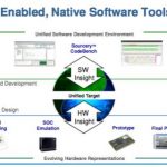
Mentor’s announcement from Design West this week pretty much signals the end of standalone ESL tools, in favor of more useful stuff. They have pulled the pieces of their Sourcery CodeBench environment along with their embedded Linux offering and their Vista virtual prototyping platform into a native embedded software development… Read More

ESD – Key issue for IC reliability, how to prevent?
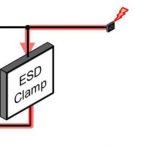
It’s a common electrical rule that when large amount of charge gets accumulated, it tries to break any of its surrounding isolation. Although it wouldn’t have been prominent in 1980s or 90s, protection for ICs from such damaging effects is a must, specifically in large mixed-signal designs of today, working at different voltages… Read More
Mentor Graphics’ Best User2User Ever

Calling all Mentor users! Don’t forget to register for the U2U in San Jose on Thursday, April 25.
In addition to three worthy keynotes, you will find a more interactive and solution-focused day than in the past. There are sessions on place & route, custom/AMS, emulation, test and yield analysis, functional verification, Calibre… Read More
Mentor’s New Embedded Strategy
If there is a trend I can detect in verification in 2013, it is taking verification environments and making the user interface, scripts, and tools work uniformly across the whole spectrum of possible verification “substrates” from virtual platforms, FPGA boards, emulation, actual chips, RTL simulation and so … Read More
Wally Rhines: Embedded Software the Next Revolution?
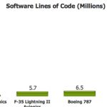
As seems to be traditional, Wally Rhines gave a keynote here at the GlobalPress Electronics Summit here in sunny Santa Cruz. It was entitled Embedded Software, the Next Revolution in EDA. Unlike Cadence and Synopsys, Mentor has a strong position in embedded software. It has been build up over a long time through a series of acquisitions… Read More
Chasing DP Rabbits
“Now, here, you see, it takes all the running you can do, to keep in the same place. If you want to get somewhere else, you must run at least twice as fast as that!”
—Lewis Carroll, Through the Looking Glass
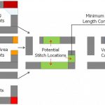
The use of stitching can greatly reduce the number of double patterning (DP) decomposition violations that a designer has to resolve.… Read More
Mentor U2U, Not Your Father’s User Conference

I talked to Michael Buehler-Garcia about the changes Mentor is making to U2U, their user conference. It is in San Jose on April 25th at the DoubleTree.
Firstly, there are 3 great keynotes, two of whom I’ve seen speak before and can unreservedly recommend. Unfortunately I’m traveling that week and won’t be able… Read More
Cutting the Key to 14nm Lithography
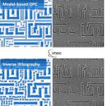
It appears that immersion lithography is now the plan of record for manufacturing ICs at 14nm. How is it possible to use 193nm wavelength light at 14nm? How can we provide the process window to pattern the such tight pitches? The secret lies in computational lithography. For 20nm, the two key innovations in computational lithography… Read More
Mentor Graphics User2User Conference

April 25, 2013, San Jose, CA
Click here to register.
Come hear Mentor Graphics CEO, Wally Rhines, 2013 Kaufman Award Winner,Chenming Hu, and Xilinx Senior VP,Victor Peng, at the User2User Conference in San Jose.
KEYNOTES
Organizing by Design
9:00am – 9:50am
Walden C. Rhines | CEO & Chairman | Mentor Graphics
Winning products… Read More
For power and performance, Fins or BOXes?
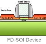
I recently spoke to Arvind Narayanan, Product Marketing Manager for Mentor’s place and route division about emerging technology. This of course led to FinFETS, FDSOI, performance, power, and cost-benefit. The battle between FDSOI and FinFETs, said Narayanan, is going to be something to watch.
Both FDSOI and FinFET technologies… Read More