You are currently viewing SemiWiki as a guest which gives you limited access to the site. To view blog comments and experience other SemiWiki features you must be a registered member. Registration is fast, simple, and absolutely free so please,
join our community today!
WP_Term Object
(
    [term_id] => 157
    [name] => EDA
    [slug] => eda
    [term_group] => 0
    [term_taxonomy_id] => 157
    [taxonomy] => category
    [description] => Electronic Design Automation
    [parent] => 0
    [count] => 4443
    [filter] => raw
    [cat_ID] => 157
    [category_count] => 4443
    [category_description] => Electronic Design Automation
    [cat_name] => EDA
    [category_nicename] => eda
    [category_parent] => 0
    [is_post] =>
)
How many languages an Engineer should speak?by ahmed.shahein on 06-08-2012 at 9:37 amCategories: EDA
I speak VHDL and SystemC, others speak Verilog and SystemVerilog … what do you speak?
Before getting into the core of the topic let me give you some round figures, engineers love numbers. Julian Lonsdale “European Sales Manager at Aldec” informed me at the Xfest Munich last month that Aldec carried out a survey to evaluate the usage… Read More
Okay, President Obama didn’t actually stop at DAC but he did do a drive by. I happened to be stepping out for some much needed fresh air and there goes his speeding motorcade. It was quite a sight actually, with all of the motorcycles, SUVs, a SWAT vehicle and even a paramedic rig (my son the Fireman drives one of those). The president … Read More
Partitioning Panelby Paul McLellan on 06-06-2012 at 4:53 pmCategories: EDA, Events
I moderated a panel on partitioning today and I have to say that I learned some things. The panelists were Jonathan DeMent from IBM, Santosh Santosh from NVIDIA and Hao Nham of eSilicon. Considering the different types of designs being done their approach to partitioning and the reasons for doing so were very similar.
When you first… Read More
Wednesday morning I attended a panel discussion with: ARM, IBM, Cadence, GLOBALFOUNDRIES and Samsung.
The panelists all sang the same song of collaboration between EDA, IP and Foundry to enable 28nm, 20nm and even 14nm.… Read More
Today at DAC Belle Wei received the Marie Pistilli Award, presented to her by Patrick Groeneveld the DAC chair (and flowers from DAC via Chi-Foon Chan, now co-ceo of Synopsys). She was then interviewed by Daya Nadamuni.
Her father was a military general in China and in 1949 in the revolution her family fled to Taiwan where she was born.… Read More
I arrived to a sunny San Francisco this afternoon, checked into my hotel then visited Moscone Center to pick up my Independent Media credentials. On the walk over I passed by Yerba Buena Gardens.… Read More
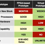
There are two main approaches to building a substructure on which to do software development and architectural analysis before a chip is ready: virtual platforms and FPGA prototyping.
Virtual platforms have the advantage that they are fairly quick to produce and can be created a long time before RTL design for the various blocks… Read More
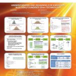
On Wednesday there is a User Track Poster Session that examines the design impact of process variation in GLOBALFOUNDRIES 28nm technology. For those of you who are wondering what process variation looks like at 20nm take this 28nm example and multiply it by one hundred (slight exaggeration, maybe).
Variation effects have a significant… Read More
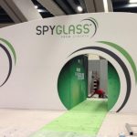
Spyglass by Atrentaby Paul McLellan on 06-03-2012 at 4:27 pmCategories: EDA
I’ve been helping get booths set up at DAC in Moscone for the last couple of days. Atrenta’s booth shows their new branding that I talked about last week. Now you can see what they are doing in this picture of their booth. As I sort of guessed they are leading with the Spyglass name. The booth says everywhere “Spyglass… Read More
I blogged several times over the last few weeks about places in San Francisco other than DAC at the Moscone Center. Since they are now spread all over the site it is not so easy to find them. So here they are again all in one place.
Places to eat and drink near the Moscone center
Interesting San Francisco bars
Where to get the best coffee… Read More







Musk’s Orbital Compute Vision: TERAFAB and the End of the Terrestrial Data Center