You are currently viewing SemiWiki as a guest which gives you limited access to the site. To view blog comments and experience other SemiWiki features you must be a registered member. Registration is fast, simple, and absolutely free so please,
join our community today!
WP_Term Object
(
    [term_id] => 157
    [name] => EDA
    [slug] => eda
    [term_group] => 0
    [term_taxonomy_id] => 157
    [taxonomy] => category
    [description] => Electronic Design Automation
    [parent] => 0
    [count] => 4534
    [filter] => raw
    [cat_ID] => 157
    [category_count] => 4534
    [category_description] => Electronic Design Automation
    [cat_name] => EDA
    [category_nicename] => eda
    [category_parent] => 0
    [is_post] =>
)
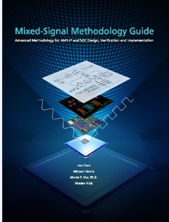
Almost every SoC has multiple analog blocks so AMS methodology is an important topic to our growing electronics industry. Authored by Jess Chen (Qualcomm), Michael Henrie (Cliosoft), Monte Mar (Boeing) and Mladen Nizic (Cadence), the book is subtitled: Advanced Methodology for AMS IP and SoC Design, Verification and Implementation… Read More
Almost every SoC has multiple analog blocks so AMS methodology is an important topic to our growing electronics industry. Authored by Jess Chen (Qualcomm), Michael Henrie (Cliosoft), Monte Mar (Boeing) and Mladen Nizic (Cadence), the book is subtitled: Advanced Methodology for AMS IP and SoC Design, Verification and Implementation… Read More
When I worked for virtual platform companies, one of the things that I used to tell prospective customers was that virtual prototypes were not some second-rate approach to software and hardware development to be dropped the moment real silicon was available, that in many ways they were better than the real hardware since they had… Read More
Synopsys announced their results today. With Magma rolled in (but not yet SpringSoft since that hasn’t technically closed) they had revenue of $443M up 15% from $387M last year. This means that they are all but a $1.75B company and a large part of the entire EDA industry (which I think of as being $5B or so, depending on just what… Read More
Cadence at 20nmby Paul McLellan on 08-21-2012 at 8:10 pmCategories: Cadence, EDA
Cadence has a new white paper out about the changes in IC design that are coming at 20nm. One thing is very clear: 20nm is not simply “more of the same”. All design, from basic standard cells up to huge SoCs has several new challenges to go along with all the old ones that we had at 45nm and 28nm.
I should emphasize that the paper… Read More
In the early 1980s the ideas and infrastructure for what would eventually be called ASIC started to come together. Semiconductor technology had reached the point that a useful number of transistors could be put onto a chip. But unlike earlier, when a chip only held a few transistors and thus could be used to create basic generic building… Read More
A Brief History of Mentor Graphicsby Beth Martin on 08-20-2012 at 11:00 pmCategories: EDA, Siemens EDA
In 1981, Pac-Man was sweeping the nation, the first space shuttle launched, and a small group of engineers in Oregon started not only a new company (Mentor Graphics), but an entirely new industry, electronic design automation (EDA).
Mentor founders Tom Bruggere, Gerry Langeler, and Dave Moffenbeier left Tektronix with a great… Read More
I was very happy to see that Cadence has decided to hold MEMCON again in 2012, in Santa Clara on September 18[SUP]th[/SUP] . The session will start with “New Memory Technologies and Disruptions in the Ecosystem”from Martin Lund.
Martin is the recently (March this year) appointed Senior VP for the SoC Realization Group at cadence:… Read More
A Brief History of SoCsby Daniel Nenni on 08-19-2012 at 10:00 amCategories: EDA
Interesting to note; our cell phones today have more computing power than NASA had for the first landing on the moon. The insides of these mobile devices that we can’t live without are not like personal computers or even laptops with a traditional CPU (central processing unit) and a dozen other support chips. The brain, heart, and… Read More
When I think of EDA companies the first geography that comes to mind is Silicon Valley because of the rich history of semiconductor design and fabrication, being close to your customers always makes sense. In the information era it shouldn’t matter so much where you develop EDA tools, so there has been a gradual shift to a wider… Read More


Enhancing Multi-Domain System Simulation with FMI Co-Simulation