You are currently viewing SemiWiki as a guest which gives you limited access to the site. To view blog comments and experience other SemiWiki features you must be a registered member. Registration is fast, simple, and absolutely free so please,
join our community today!
WP_Term Object
(
    [term_id] => 157
    [name] => EDA
    [slug] => eda
    [term_group] => 0
    [term_taxonomy_id] => 157
    [taxonomy] => category
    [description] => Electronic Design Automation
    [parent] => 0
    [count] => 4439
    [filter] => raw
    [cat_ID] => 157
    [category_count] => 4439
    [category_description] => Electronic Design Automation
    [cat_name] => EDA
    [category_nicename] => eda
    [category_parent] => 0
    [is_post] =>
)
I could have written the sequence of the title in reverse order, but no, design is the one which initiates the need of a particular flow and the flow needs support of EDA tools to satisfy that need. It’s okay if the design is small; some manual procedures and workarounds/scripts may be able to perform certain jobs. However, as the design… Read More
Of course if you are in the business of selling high-level synthesis (HLS) tools then the obvious answer is immediately. Start at 9am tomorrow morning. But a more realistic answer is when you are having to do something completely new. If you are working on a legacy design, perhaps with pre-existing IP, then moving the design up to … Read More
Well, Sweden is not noted for its carnivals, Brazil is not noted for it’s tall blonde blue-eyed women, Sweden’s climate is not great for growing sugar cane and Brazil’s isn’t great for reindeer. Both countries speak languages with odd-sounding vowels but they are not the same language. But, ding, Jasper… Read More
Sometimes press releases just make me scratch my head. Today’s example comes from IBM: after tying PowerPC and Power.org in knots for almost 20 years with rules and restrictive licensing, IBM breaks ranks and sets up ANOTHER consortium with different players.… Read More
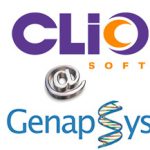
GenApSys is a biotech company developing proprietary DNA sequencing technology. As part of that they develop their own custom sequencing chips. These have an analog component and like many people they use the Cadence Virtuoso analog design environment for this.
I talked to Hamid Rategh who is GenApSys’s VP engineering.… Read More
Founders
The founder, Ghislain Kaiser, spent about 10 years at STMicroelectronics, mainly in multimedia groups and for the wireless market. At this time, he was a power expert and tasked with making the chips use less power. The first thing he did was to look at what tools existed on the market. They wanted to use off the shelf tools… Read More
The tech standards cycle almost always goes like this: Problems or limits develop with the existing way of doing things. Innovators attempt to engineer solutions, usually many of them. Chaos ensues when customers figure out nothing new works with anything else. Competitors sit down and agree on a specification where things work… Read More
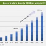
Last year, I said that the launch of ARC based complete sound system IP by Synopsys ring the bell for the opening of a new IP market segment, the “Subsystem IP”. This week, Synopsys has announced the availability of the DesignWare® Sensor IP Subsystem, a complete and integrated hardware and software solution for sensor control applications.… Read More
Through my contacts at SemiWiki I was introduced to a mixed signal IP company named SilabTech, and then decided to interview the founder and CEO, Sujoy Chakravarty.
Sujoy Chakravarty, CEO and Founder
… Read More
A SemiWiki member mentioned CircuitLaba few months back so I took a look at it today and share my first impressions.… Read More


Musk’s Orbital Compute Vision: TERAFAB and the End of the Terrestrial Data Center