In the past year, seeing the kinds of wearables doing what Smartphones can do, I wasn’t much excited about wearables; however after looking at what Intelhas demonstrated in CES 2015, a button sized SoC called Curie, I get to believe that it will be a game changer in wearables and would let Intel do what it couldn’t do with Smartphone… Read More

Electronic Design Automation
Mentor Moves to Enter IoT Fray
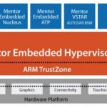
In December I signed up for an IoT “lunch and learn” hosted by Mentor Graphics. There were a number of surprising things about the session. The first and most obvious is that it was really a “breakfast-to-lunch and learn”. Starting at 9AM and going through the end of lunch, it was packed full of ‘learning.’ It was also packed full of … Read More
Coventor Panel at IEDM Digs into Variation Issues
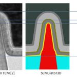
Recently I attended a panel discussion on variability in semiconductor fabrication hosted by Coventor in conjunction with the IEEE IEDM conference in San Francisco. The IEEE bills the conference as “the world’s pre-eminent forum for reporting technological breakthroughs in the areas of semiconductor and electronic device… Read More
Prototyping Kits to Accelerate IP Development & Integration into SoCs

With growing SoC size, complexity, software and hardware content in it and shrinking time-to-market, the SoC design completion in time has become increasingly dependent on IP which need to be sourced (internally or externally), customized according to the design need and integrated together into the SoC. While IP providers… Read More
Facts Support New Emergence in Semiconductor Landscape
As we left an exciting year 2014 which is poised to record 7+ % increase in semiconductor revenue (~ $338 B) compared to 2013 (~ $315 B) and entered into another promising year 2015 for semiconductors, I looked back over the year bygone and collected inferences from some of the major important events which clearly convey how 2015 can… Read More
WLAN Design Optimization at Lantiq
Right now I’m typing on my MacBook Pro computer connected to the Internet through WiFi, thanks to the electronics in both my laptop and WiFi router. I kind of take WiFi for granted because it is so ubiquitous throughout my daily life, yet there are IC designers at companies like Lantiq Semiconductorthat have to design and optimize… Read More
SoCs should invest in a strong cache position
Like most technology firms, Apple has been home to many successes, and some spectacular defeats. One failure was Project Aquarius. At the dawn of the RISC era, before ARM architecture was “discovered” in Cupertino, engineers were hunkered over a Cray X-MP/48. The objective was to design Apple’s own quad core RISC processor to … Read More
ANSYS Updates RedHawk for FinFET Nodes
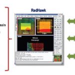
Most designers are not using FinFETs yet, however the increased transistor density and power advantages they offer are compelling. Smaller feature sizes have been a consistent driver in semiconductor technology. Eventually the market will move more and more to FinFET processes, increasingly leaving behind planar transistors.… Read More
Top Ten Semiconductor CEOs in 2014!
Since my blog about the Intel CEOs went over so well (sarcasm) I thought I should write more about semiconductor chief executive officers. This list comes from David Manners of Electronics Weekly who, unlike me, is a real journalist. Using David’s list as a starting point I will add more candidates at the end and please add yours in… Read More
Op-amps moving toward zero-drift, greater voltage range
Operational amplifiers, which are among the most widely used analog components found in nearly all types of electronic systems, are migrating toward zero-drift capability and much-greater range of voltages at the supplies and the inputs. Take Linear Technology Corp.’s LTC2057HV, a zero-drift operational amplifier, which… Read More
Enhancing Multi-Domain System Simulation with FMI Co-Simulation