You are currently viewing SemiWiki as a guest which gives you limited access to the site. To view blog comments and experience other SemiWiki features you must be a registered member. Registration is fast, simple, and absolutely free so please,
join our community today!
WP_Term Object
(
    [term_id] => 157
    [name] => EDA
    [slug] => eda
    [term_group] => 0
    [term_taxonomy_id] => 157
    [taxonomy] => category
    [description] => Electronic Design Automation
    [parent] => 0
    [count] => 4441
    [filter] => raw
    [cat_ID] => 157
    [category_count] => 4441
    [category_description] => Electronic Design Automation
    [cat_name] => EDA
    [category_nicename] => eda
    [category_parent] => 0
    [is_post] =>
)
Six years ago I first interviewed Stephen Crosher, CEO and Co-founder of Moortecas they were in startup mode with some new semiconductor IP for temperature sensing, and earlier this month I attended their webinar all about embedded in-chip monitoring to get caught up with their technology and growing success. Ramsay Allen is … Read More
Aldec continues to claim a bigger seat at the table, most recently in their attendance at SC17, the supercomputing conference hosted last month in Denver. I’m really not sure how to categorize Aldec now. EDA company seems to miss the mark by a wide margin. Prototyping company? Perhaps, though they have a much stronger focus on end-applications… Read More
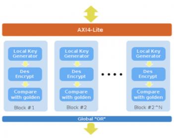
With the advent of the Internet-of-Things (IoT), Industry 4.0, Cognitive Computing, and autonomous vehicles and robots we are seeing an unprecedented number of systems-on-a-chip (SoCs) going into mission-critical applications. To accomplish the complexity of these applications, SoCs are being manufactured in leading-edge… Read More
The year is now 1991 and in search for a more peaceful life we decided to move to Canada. At that time, very few companies had advanced flows in VLSI but Ottawa having BNR, Northern Telecom, Mitel, etc., looked to be the most promising place. After a few hiccups in finding a job, I landed in MOSAID, a small company with35 people at that … Read More
I recently was introduced to a white paper written by John Stabenow, Director at Mentor, a Siemens Business, that gave an excellent overview of things to consider before launching into the design of an IoT edge project. John starts the paper with a quote from Pliny the Elder (A.D.23-A.D.79) who said, “The best plan is, as the common… Read More
The Consumer Electronics Show (CES) is in its 50th year believe it or not! The first one was in New York (1967) with 250 exhibitors and 17,500 attendees. Portable radios and TVs were all the rage followed by VCRs in 1970 and camcorders and compact discs in 1981. This year there will be 3,900+ exhibits and an estimated 170,000 attendees… Read More
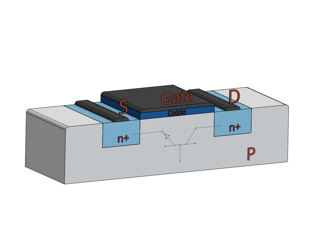
Terms like avalanche breakdown and impact ionization sound like they come from the world of science fiction. They do indeed come from a high stakes world, but one that plays out over and over again here and now, on a microscopic scale in semiconductor devices – namely as part of electrostatic discharge (ESD) protection. Semiconductor… Read More
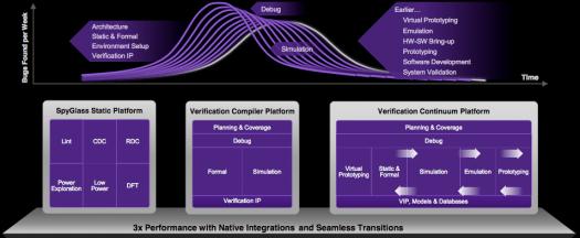
Unless you have been living in a cave for the last several years, by now you know that “Shift Left” is a big priority in product design and delivery, and particularly in verification. Within the semiconductor industry I believe Intel coined this term as early as 2002, though it seems now to be popular throughout all forms of technology… Read More
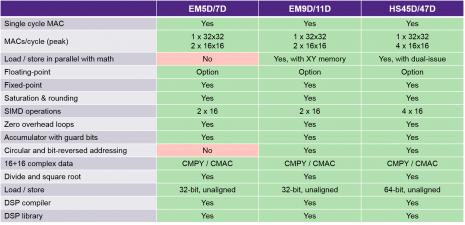
Synopsys DesignWareARC HS4xD family is a perfect example of high performance DSP, enhanced RISC CPU IP core, able to address high-end IoT, mid to high-end audio or baseband control. ARC HS4xD architecture is 10-stage pipeline for high Fmax, resulting in excellent RISC efficiency with 5.2 CoreMark per MHz. ARC EMxD processors… Read More
I recently wrote an article about Synopsys’ DesignWare Security IP for the Internet-of-Things market and was interested to see that a startup, Starblaze Technology, has now used parts of the same IP in its latest Solid-State Drive (SSD) controller. The security IP caught my eye, but the rest of the story really put things into focus.… Read More


Musk’s Orbital Compute Vision: TERAFAB and the End of the Terrestrial Data Center