You are currently viewing SemiWiki as a guest which gives you limited access to the site. To view blog comments and experience other SemiWiki features you must be a registered member. Registration is fast, simple, and absolutely free so please,
join our community today!
WP_Term Object
(
    [term_id] => 157
    [name] => EDA
    [slug] => eda
    [term_group] => 0
    [term_taxonomy_id] => 157
    [taxonomy] => category
    [description] => Electronic Design Automation
    [parent] => 0
    [count] => 4441
    [filter] => raw
    [cat_ID] => 157
    [category_count] => 4441
    [category_description] => Electronic Design Automation
    [cat_name] => EDA
    [category_nicename] => eda
    [category_parent] => 0
    [is_post] =>
)
I attend a lot of events on machine learning and write about it regularly. However, I learned some exciting new information about machine learning in a very surprising place recently. Every year for the last few years I have attended the HSPICE SIG dinner hosted by Synopsys in Santa Clara. This event starts with a vendor fair featuring… Read More
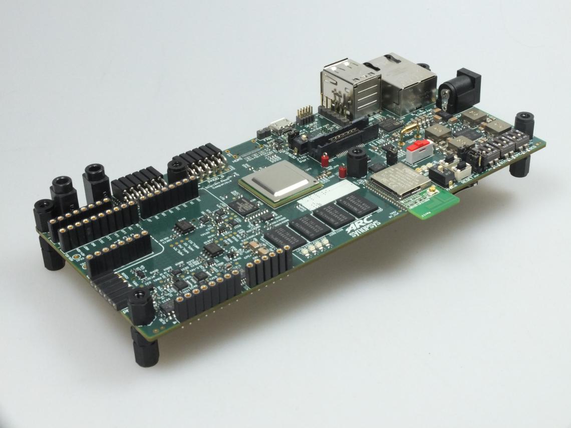
When I think of an IP development kit, I imagine software plus a hardware model I can run on a prototyper or, closer to the kits offered by semi companies, software plus a board hosting an FPGA implementation of the IP along with DDR memory, flash and a variety of interfaces. These approaches work well for IP providers because hardware… Read More
In case you missed the TSMC event, ANSYS and TSMC are going to reprise a very important topic – signing-off reliability for ADAS and semi-autonomous /autonomous systems. This topic hasn’t had a lot of media attention amid the glamor and glitz of what might be possible in driverless cars. But it now seems like the cold light of real … Read More
How could we differentiate between deep learning and machine learning as there are many ways of describing them? A simple definition of these software terms can be found here. Let’s look into Artificial Intelligence (AI), which was coined back in 1956. The term AI can be defined as human intelligence exhibited by machines.… Read More
I am very sorry but I have to break the flow of sharing initiatives, to reiterate the reason for these articles and maybe amplify the message these articles should promote.
I got a few inquiries from LinkedIn connections, who read the previous articles, with a very interesting point of view. This proves that after 5 articles some … Read More
I’ve been driving cars since 1975 and in the early days we had simplistic gauges for feedback like: Speed, Fuel level, Oil level, RPM. Back then when you popped the hood of a car you could see through the engine compartment onto the ground below, however with today’s cars the engine compartments are crammed with tubes,… Read More
There is a trend among design companies to want to extract more intelligence, from designs in-process and designs past, in support of optimizing total enterprise efficiency. Design automation companies see opportunity in leveraging this interest since they, in various ways, have a handle on at least part of the underlying data.… Read More
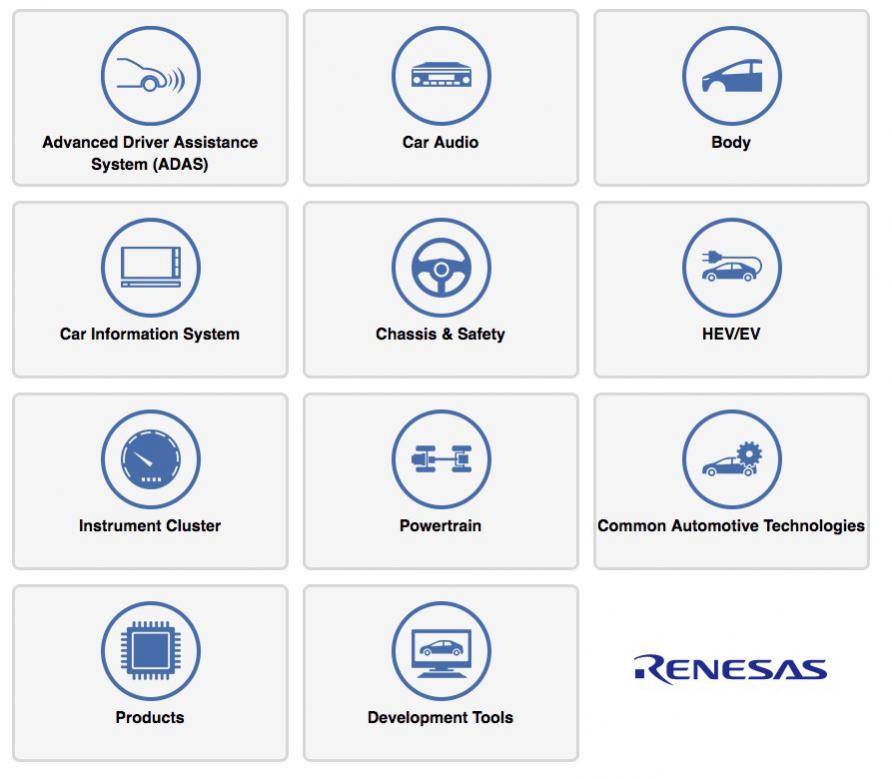
I come from a car-centric family where my father actually bought and sold over 300 vehicles in his lifetime, so automotive mega-trends pique my interest. A new conference called Semiconductors ISO 26262 held it’s first annual event last month, meeting in Munich with guest speakers from some impressive companies like: … Read More
If you’re in the ASIC business, by now you should have a rough understanding of ISO 26262, the safety standard for automotive electronics. You may be less familiar with DO-254 which has somewhat similar intent for airborne electronics. Unless, that is, you design with FPGAs in which case your familiarity may be the other way around… Read More
Until recently, ICs at bleeding edge nodes like 7nm technology from foundries like TSMC were mostly targeted for high-performance-computing (HPC) and mobile applications or possibly high radix switches that needed the increased performance of advanced nodes. The momentum of Moore’s law and Moore-than-Moore saw foundries… Read More


Musk’s Orbital Compute Vision: TERAFAB and the End of the Terrestrial Data Center